Microscope
Items labeled can be shared by non-NIMS users. For details, please refer to the related links in the description column of each equipment/facility.
Cs corrected Scanning Transmission Electron Microscope: Spectra Ultra S/TEM
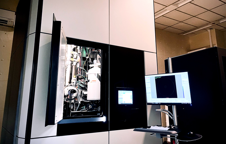

Cs corrected Scanning Transmission Electron Microscope: Spectra Ultra S/TEM
The SpectraUltra system can be operated at different voltages (30 ~ 300 kV) in a single microscopy session, and has 4.45 srad EDS solid angle (4.04 srad solid angle with an analytical double tilt holder).
Deep UV laser-assisted 3D atom probe : Invizo6000
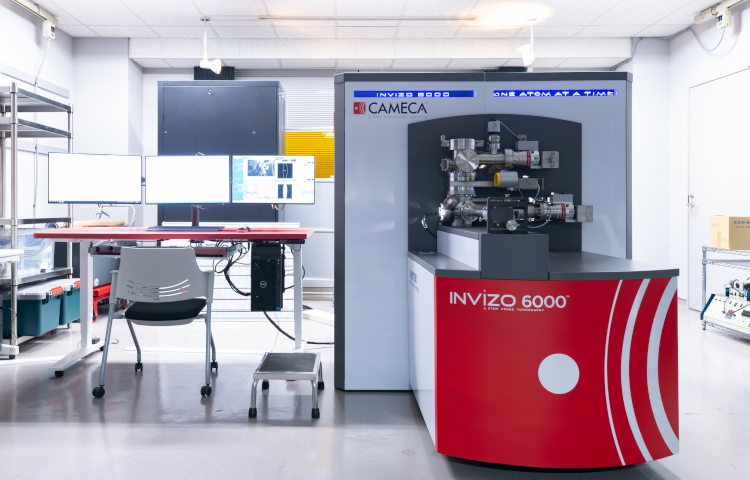

Deep UV laser-assisted 3D atom probe : Invizo6000
3D Atom Probe : LEAP5000XS
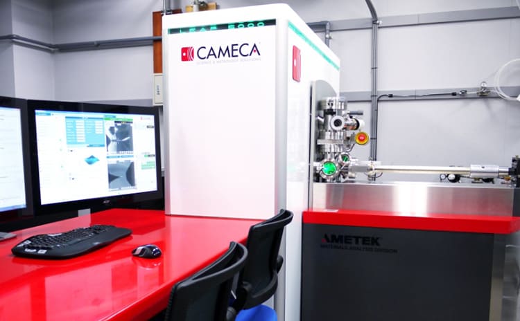

3D Atom Probe : LEAP5000XS
The 3D atom probe method can detect and identify the position of single atoms including light elements, which are difficult to observe with electron microscopes. It is also very effective in analyzing the distribution of elements within a variety of materials or devices.
X-ray CT
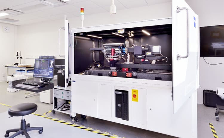

X-ray CT
X-ray CT provides crisp image quality due to its high resolution and high contrast. The three-dimensional detailed structure of battery materials can be evaluated in a non-destructive manner over a range from sub-micron to millimeter order. In addition, the changes in battery electrode structures during charging and discharging can also be observed.
The Periscopic Confocal Microscope for in-situ observation under High Magnetic Fields
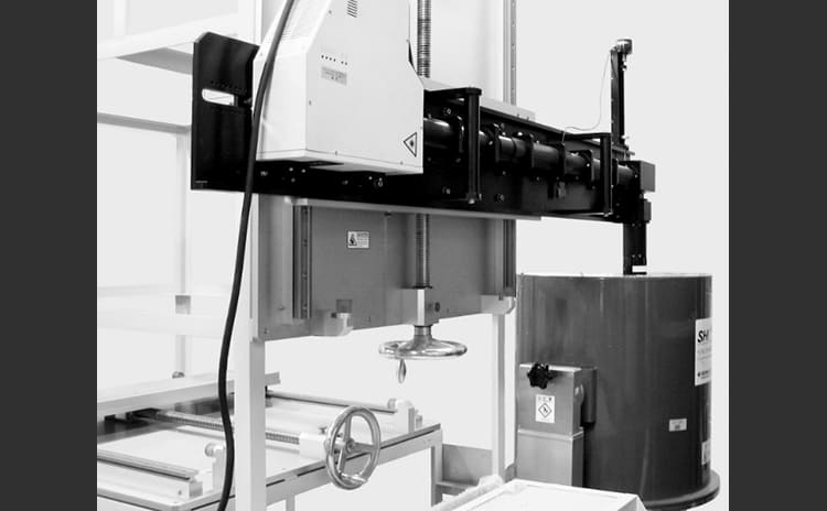

The Periscopic Confocal Microscope for in-situ observation under High Magnetic Fields
This periscopic confocal microscope realizes an in-situ microscopic observation even under high magnetic fields up to 13 T. The resolution obtained is several hundreds of nanometers. This system can be used to investigate the mechanisms of magnetic field effects on various processes.
Cathodoluminescence spectral imaging system
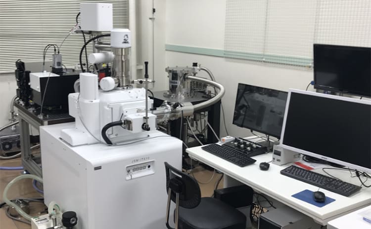

Cathodoluminescence spectral imaging system
With nano-level spatial resolution, this system is possible to obtain emission images and emission spectra of a microscopic region of samples with high sensitivity from ultraviolet to near-infrared wavelength. In addition, it is equipped with a function for hyper spectral image, which can measure both cathodoluminescence images and spectra at one time.
High Temperature, High magnetic field Time Resolved Magneto-Optical Kerr Effect (TR-MOKE) measurement system
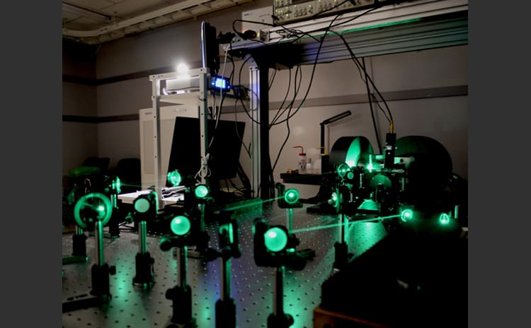

High Temperature, High magnetic field Time Resolved Magneto-Optical Kerr Effect (TR-MOKE) measurement system
TR-MOKE system is designed to measure magnetization dynamics. The magnetization state is excited by a pump beam and the magneto-optical Kerr signal is detected by probe beam with some time delay. This is the unique system in the world with a maximum magnetic field of 7 T and temperature of 700 K.
Real-time lock-in 3D infrared heat generation analysis system
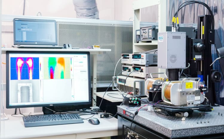

Real-time lock-in 3D infrared heat generation analysis system
This system enables ultrasensitive imaging measurements of thermal responses generated when periodic external stimuli (e.g., charge current, electric field, magnetic field, heat, light, and strain) are applied to materials or devices. Using this system, NIMS has succeeded in the world's first observations of various thermoelectric effects including the anisotropic magneto-Peltier and magneto-Thomson effects.
Plasma FIB (PFIB)-SEM-Laser tri-beam for 3D microstructure analysis
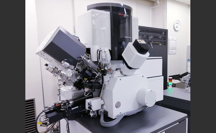

Plasma FIB (PFIB)-SEM-Laser tri-beam for 3D microstructure analysis
This is a scanning electron microscope (SEM)-based microscope designed to observe the microstructure of materials with high resolution and three dimensions. It can obtain three-dimensional information on microstructure, composition, crystal orientation, etc. in a large volume as large as sub-millimeter with high resolution, which is not possible with conventional FIB which is based on gallium liquid metal ion source.
Plasma Focused Ion Beam Scanning Electron Microscope
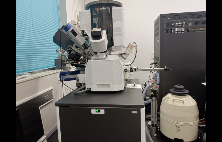

Plasma Focused Ion Beam Scanning Electron Microscope
High-Resolution Transmission Electron Microscope
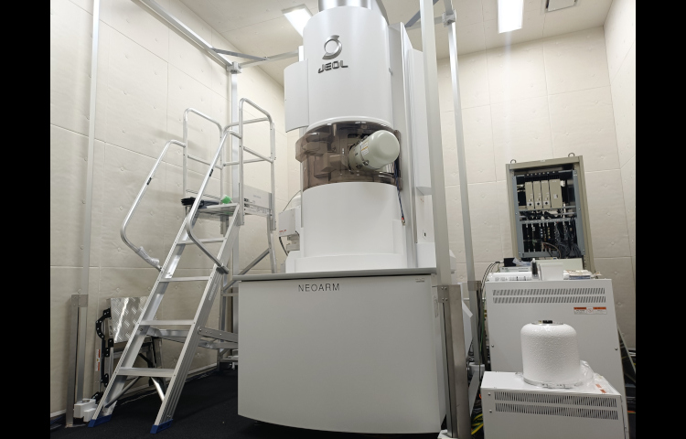

High-Resolution Transmission Electron Microscope
Scanning Transmission Electron Microscope with Microcalorimeter EDS
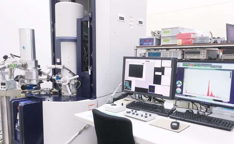

Scanning Transmission Electron Microscope with Microcalorimeter EDS
This scanning transmission electron microscope (STEM) is equipped with a microcalorimeter-type superconducting X-ray detector whose sensitivity and elemental discrimination ability are an order of magnitude higher than those of conventional detectors. This world's first application of a superconducting X-ray detector on a STEM has enabled compositional analysis of local areas with quite high accuracy.
Atomic-resolution analytical electron microscope
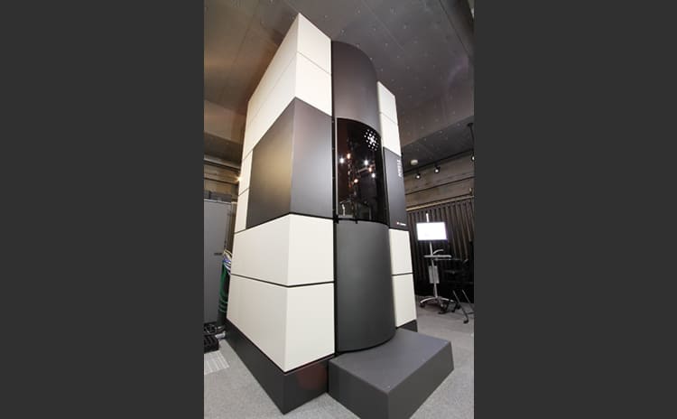

Atomic-resolution analytical electron microscope
This transmission electron microscope is equipped with two spherical-aberration correctors and a monochromator for direct observation of atomic arrangements. High-resolution TEM and scanning transmission electron microscope (STEM) imaging, Lorentz microscopy, 4D-STEM and electron energy loss spectroscopy (EELS) are available.
Low temperature scanning tunneling microscope with 16T superconducting magnet
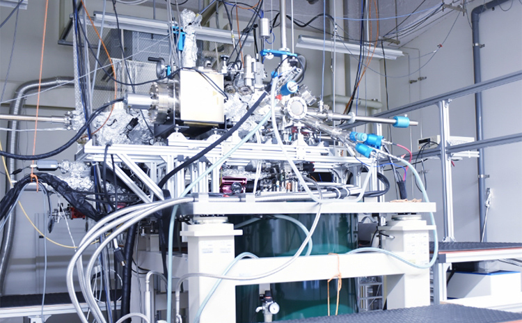

Low temperature scanning tunneling microscope with 16T superconducting magnet
This scanning tunneling microscope is used to measure the electronic states of surfaces at the atomic level. The sample temperature can be maintained at 0.4 K for up to 6 days, allowing stable and precise tunneling spectroscopic imaging with a high energy resolution of 100 µeV. It is also equipped with a superconducting magnet capable of applying high magnetic fields of up to 16 T.
Low-Temperature Ultrahigh Vacuum Scanning Probe Microscopy System
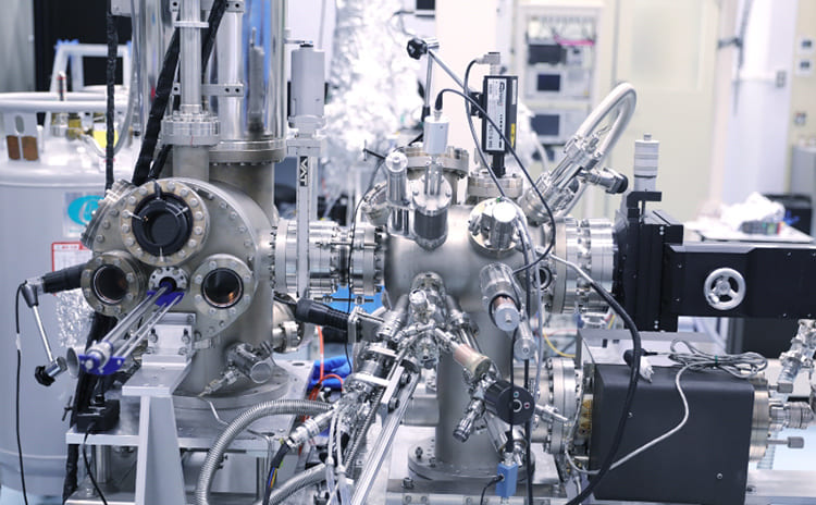

Low-Temperature Ultrahigh Vacuum Scanning Probe Microscopy System
This high-resolution scanning probe microscopy system, operating under ultrahigh vacuum conditions at 4.3 K for more than 120 hours, was specially designed for on-surface chemistry. This system is equipped with various devices for sample preparations and allows us to study single molecules. Through rich collaborations with organic chemists, this system has produced various interesting results.
Analytical Transmission Electron Microscope (JEM-ARM300F)
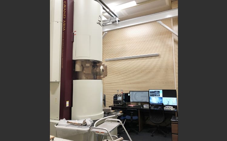

Analytical Transmission Electron Microscope (JEM-ARM300F)
This S/TEM is a world-class observation and analysis microscope equipped with double correctors and high-performance detectors. It can detect ultra-trace elements with a high-sensitivity EDS and perform in-situ observation and material property evaluation with a high-speed, high-sensitivity camera and special holder.
