Main Equipment and Facilities
2026.06.08 Update
Equipment and Facilities Supporting NIMS' Research Capabilities
The world-class research results produced by NIMS are supported by a number of excellent instruments and facilities. This page introduces some of the most advanced instruments and facilities at NIMS, including NIMS’ original instruments that are unique to our institution.
Items labeled can be shared by non-NIMS users. For details, please refer to the related links in the description column of each equipment/facility.
1. Microscope (18 items incl. 3 items updated)
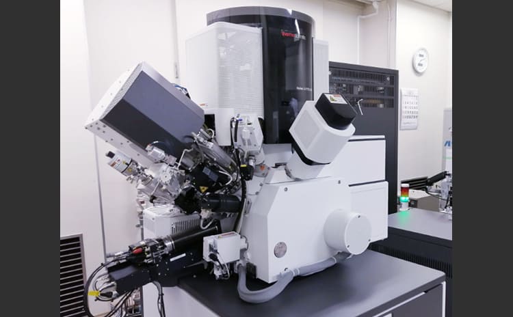
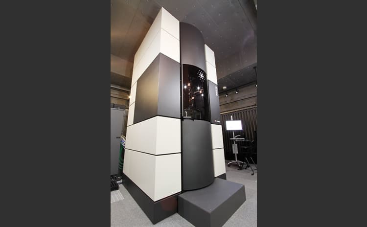
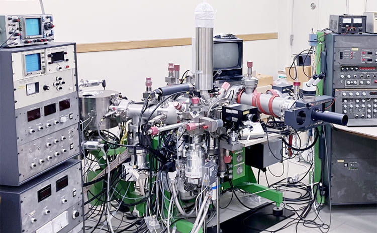
原子レベル元素分布・構造解析用透過電子顕微鏡: Spectra Ultra S/TEM
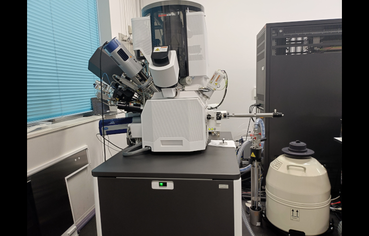
深紫外レーザーアトムプローブ装置 : Invizo6000
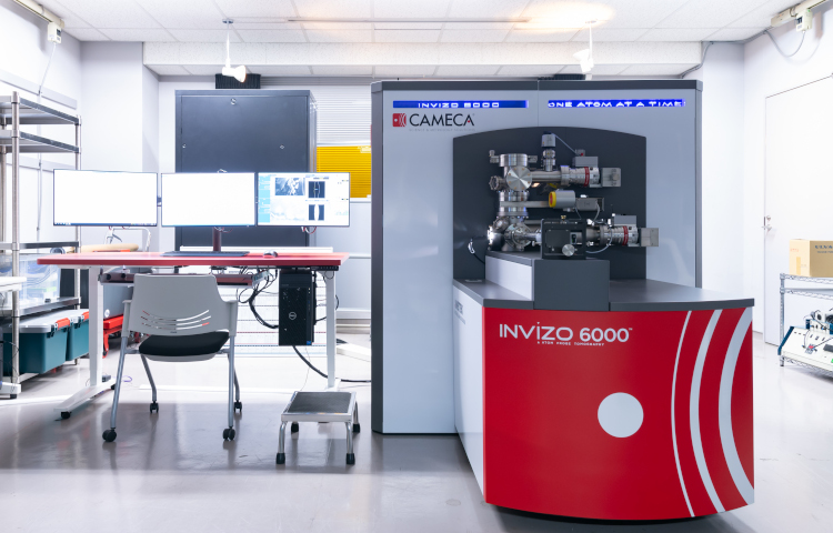
Deep UV laser-assisted 3D atom probe : Invizo6000
Atom probe tomography is the only technique that can visualize the three-dimensional distribution of atoms in materials with nearly atomic spatial resolution and high chemical sensitivity. It has an ultra wide field of view owing to new designed flight path and dual-beam deep UV laser pulse system, allowing in a greater analysis volume.
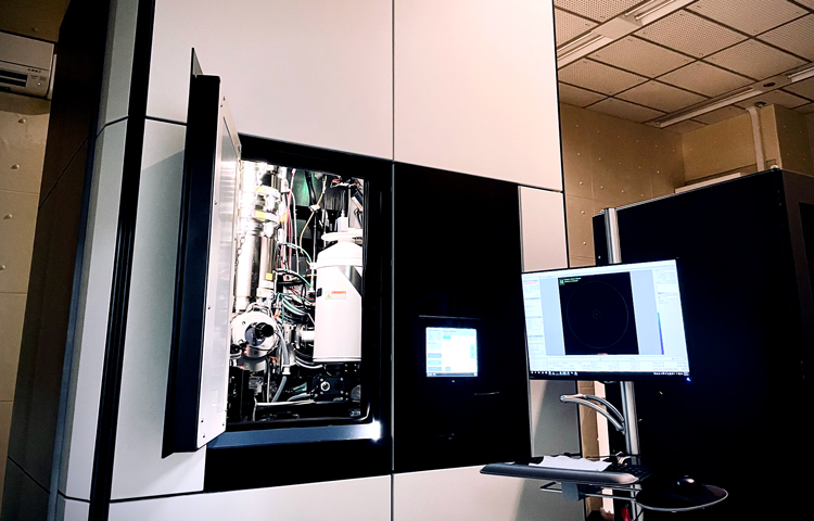
 高速データ取得型超低損傷・動的観察顕微鏡システム
High-Speed Data Acqusition Ultra-Low dose dynamic observation microscopy
Equipped with the latest aberration corrector, an ultrafast and highly sensitive pixelated STEM detector, and an ultra-high sensitivity TEM detector, it is possible to acquire large amounts of data in a short period of time. By reconstructing sample information from the vast amounts of data obtained, it becomes possible to observe materials that were previously difficult to analyze.
4D走査透過型電子顕微鏡
マルチモーダル分析電子顕微鏡
Multimodal Analytical Electron Microscope
It operates with the intuitive ease of an SEM, eliminating the need for tedious alignments. The system features four SDDs for atomic-resolution EDS mapping and a segmented STEM detector for DPC imaging. Furthermore, its highly stable stage enables TEM/EDS tomography with unmatched ease compared to conventional systems, powerfully supporting a wide variety of data collection.
X線コンピュータ断層撮影装置

X-ray CT
X-ray CT provides crisp image quality due to its high resolution and high contrast. The three-dimensional detailed structure of battery materials can be evaluated in a non-destructive manner over a range from sub-micron to millimeter order. In addition, the changes in battery electrode structures during charging and discharging can also be observed.
強磁場中その場観察装置
The Periscopic Confocal Microscope for in-situ observation under High Magnetic Fields
This periscopic confocal microscope realizes an in-situ microscopic observation even under high magnetic fields up to 13 T. The resolution obtained is several hundreds of nanometers. This system can be used to investigate the mechanisms of magnetic field effects on various processes.
カソードルミネッセンス 分光イメージング装置
Cathodoluminescence spectral imaging system
This system enables the acquisition of emission images and spectra from microscopic regions of samples with high sensitivity across a wide wavelength range, from ultraviolet to near-infrared. Furthermore, it incorporates a hyperspectral imaging function, allowing for the simultaneous measurement of both cathodoluminescence images and spectra.
高温高磁場・時間分解磁気光学Kerr効果 (TR-MOKE)測定システム
High Temperature, High magnetic field Time Resolved Magneto-Optical Kerr Effect (TR-MOKE) measurement system
TR-MOKE system is designed to measure magnetization dynamics. The magnetization state is excited by a pump beam and the magneto-optical Kerr signal is detected by probe beam with some time delay. This is the unique system in the world with a maximum magnetic field of 7 T and temperature of 700 K.
リアルタイムロックイン 3次元赤外線発熱解析装置

Real-time lock-in 3D infrared heat generation analysis system
This system enables ultrasensitive imaging measurements of thermal responses generated when periodic external stimuli (e.g., charge current, electric field, magnetic field, heat, light, and strain) are applied to materials or devices. Using this system, NIMS has succeeded in the world's first observations of various thermoelectric effects including the anisotropic magneto-Peltier and magneto-Thomson effects.
3D組織情報解析装置
Plasma FIB (PFIB)-SEM-Laser tri-beam for 3D microstructure analysis
This is a scanning electron microscope (SEM)-based microscope designed to observe the microstructure of materials with high resolution and three dimensions. It can obtain three-dimensional information on microstructure, composition, crystal orientation, etc. in a large volume as large as sub-millimeter with high resolution, which is not possible with conventional FIB which is based on gallium liquid metal ion source.
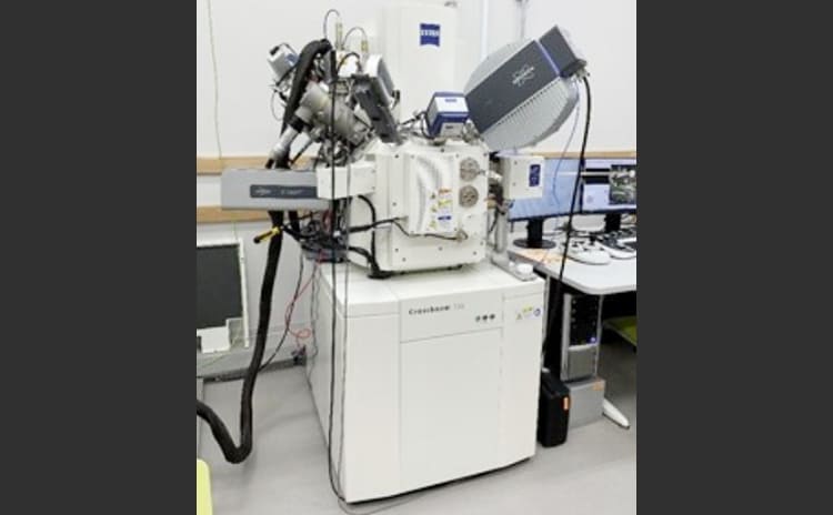
プラズマ集束イオンビーム走査電子顕微鏡
Plasma Focused Ion Beam Scanning Electron Microscope
This instrument enables three-dimensional structural analysis by continuously capturing high-resolution images of large sample cross-sections, achieved through rapid and stable milling using a plasma FIB. It also supports atmospheric non-exposure transfer and low-temperature processing of highly reactive samples, such as battery materials.
高分解能透過電子顕微鏡
High-Resolution Transmission Electron Microscope
This instrument enables comprehensive analysis of structure, composition, and chemical state at the atomic level. It supports air-tight sample transfer as well as low-dose and low-temperature observation, allowing highly precise visualization of reaction phases and fine structural changes occurring at interfaces of battery materials.
マイクロカロリメータ型 EDS搭載走査透過型電子顕微鏡
Scanning Transmission Electron Microscope with Microcalorimeter EDS
This scanning transmission electron microscope (STEM) is equipped with a microcalorimeter-type superconducting X-ray detector whose sensitivity and elemental discrimination ability are an order of magnitude higher than those of conventional detectors. This world's first application of a superconducting X-ray detector on a STEM has enabled compositional analysis of local areas with quite high accuracy.
単原子分析電子顕微鏡
Atomic-resolution analytical electron microscope
This transmission electron microscope is equipped with two spherical-aberration correctors and a monochromator for direct observation of atomic arrangements. High-speed & high-resolution TEM, scanning transmission electron microscope (STEM) imaging, Lorentz microscopy, and 4D-STEM and electron energy loss spectroscopy (EELS) are available.
極低温・高磁場走査型トンネル顕微鏡
Low temperature scanning tunneling microscope with 16T superconducting magnet
This scanning tunneling microscope is used to measure the electronic states of surfaces at the atomic level. The sample temperature can be maintained at 0.4 K for up to 6 days, allowing stable and precise tunneling spectroscopic imaging with a high energy resolution of 100 µeV. It is also equipped with a superconducting magnet capable of applying high magnetic fields of up to 16 T.
極低温超高真空走査型プローブ顕微鏡
Low-Temperature Ultrahigh Vacuum Scanning Probe Microscopy System
This high-resolution scanning probe microscopy system, operating under ultrahigh vacuum conditions at 4.3 K for more than 120 hours, was specially designed for on-surface chemistry. This system is equipped with various devices for sample preparations and allows us to study single molecules. Through rich collaborations with organic chemists, this system has produced various interesting results.
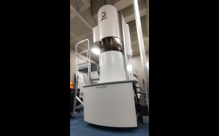
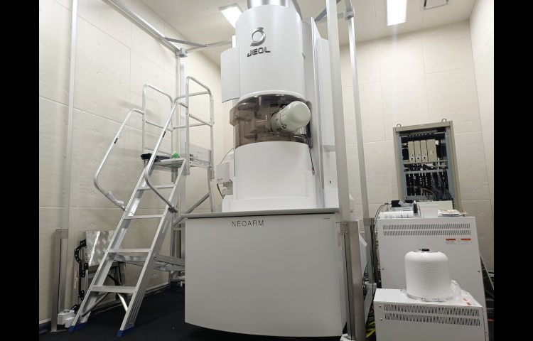
広空間・高分解能分析電子顕微鏡 (JEM-ARM300F)
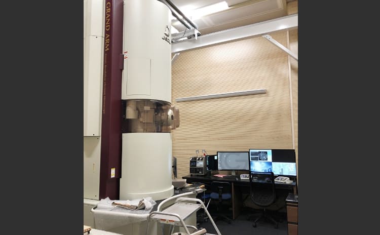
Analytical Transmission Electron Microscope (JEM-ARM300F)
This S/TEM is a world-class observation and analysis microscope equipped with double correctors and high-performance detectors. It can detect ultra-trace elements with a high-sensitivity EDS and perform in-situ observation and material property evaluation with a high-speed, high-sensitivity camera and special holder.
2. Atomic and Electronic Structure Analysis/ Trace Elements Analysis (8 items)
800MHzワイドボア 固体高分解能NMRシステム
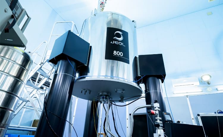
800 MHz wide bore Solid-State NMR System
High-field (18.79T) wide-bore high-resolution NMR system specialized for solid materials, which provides structural analyses for various kinds of solid materials as they are. The system is equipped with state-of-the-art NMR technology to meet the needs of various material researchers developing cutting-edge materials.
局所化学結合状態解析システム
Analysis system for probing local chemical-bonding states
A transmission electron microscope with the highest energy resolution in Japan enables spectroscopic imaging of chemical bonding states, dielectric properties, and lattice vibrations on the atomic to nano scale. Equipped with highly sensitive detectors, it is also capable of mapping trace elements and observing the structure of organic materials.
走査型硬X線光電子分光分析装置
Scanning Hard X-ray Photoelectron Spectroscopy
with a detection depth of about 20 nm with minimal influence of surface oxidation or contamination of the sample. It also supports depth analysis of organic materials using a gas cluster ion gun, non-exposure to air measurements, bias-applied measurements on samples under heating or cooling condition, and operando measurements.
硬X線光電子分光装置 (HAXPES)
Hard X-ray Photoelectron Spectroscopy (HAXPES)
HAXPES uses hard X-rays to precisely detect surface elements from depths of 10 nm or greater, and the focused Cr Kα beam enables deeper analysis than XPS. In addition, the system is directly connected to an argon atmosphere glove box, allowing samples to be transported without exposure to the atmosphere. Operando measurements for next-generation batteries are also available.
磁場偏向型2次イオン質量分析装置 : IMS-4f
Magnetic Sector Secondary Ion Mass Spectrometry : IMS-4f
This system can perform highly accurate and sensitive analysis including isotopes from hydrogen to uranium. It is mainly used for the analysis of samples treated with hydrogen isotope and oxygen isotope. The sample temperature during the analysis can be selected between room temperature and liquid nitrogen temperature.
プロトン移動反応飛行時間型質量分析計
Proton Transfer Reaction Time-of-flight Mass Spectrometer (PTR-TOF-MS)
This ultra-sensitive gas analyzer enables real-time quantitative measurement of trace gas components at ppb (parts-per-billion) and ppt (parts-per-trillion) levels. In addition to analyzing volatile compounds (odors) emitted from foods and beverages, agricultural and livestock products, fragrances and cosmetics, and industrial products, it can measure gases generated by living organisms, including humans, animals, plants, and microorganisms (e.g., breath, skin gas, and urine gas). The system contributes to the research and development of olfactory sensors (electronic nose, e-nose)for applications such as medical diagnostics, health monitoring, quality assessment, environmental monitoring, and safety and disaster prevention.
イメージング型顕微 スピン分解光電子分光装置

Imaging-type spin-resolved photoemission microscopy
This machine achieves a spatial resolution of 30 nm in photoemission spectroscopy. Imaging technique reduces the measurement time of spin-resolved photoemission spectroscopy by more than four orders of magnitude compared to conventional machines. It contributes to the development of materials and devices by visualizing the electronic states in nano scale, which has been difficult with conventional photoemission spectroscopy.
軟X線マルチモーダルオペランド顕微分光装置
Soft X-ray complete operando photoemission ultramicroscopy
This instrument leverages the high-brilliance soft X-rays at NanoTerasu to visualize electronic behavior within materials with the world’s highest spatial resolution. It enables the measurement of electronic states not only under steady-state conditions but also in realistic operating environments—a capability previously out of reach.
3. Physical Properties Measurement (9 items)
16T強磁場環境物理特性測定システム(PPMS)

16T Physical Property Measurement System (PPMS)
The PPMS is an advanced system designed to automatically measure a wide range of physical properties including magnetic, electrical and thermal characteristics up to a maximum magnetic field of 16 Tesla. With its dedicated software, it enables seamless 24-hour continuous automated measurements. The use of a specialized sample pack facilitates easy attachment of samples, ensuring effortless operation and precise results.
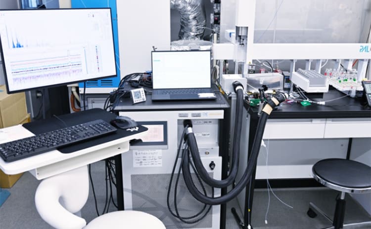
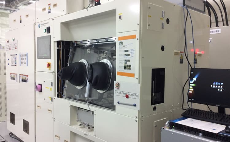
ハイスループット電解液探索システム
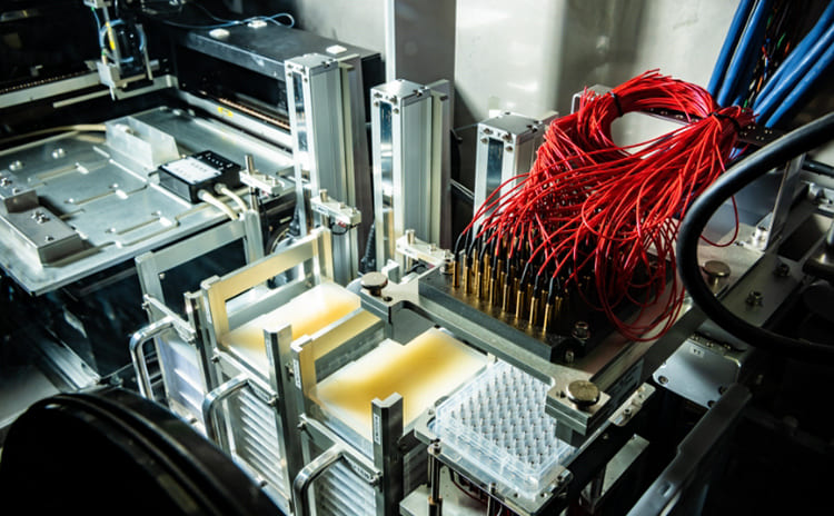
NIMS Automated Robotic Electrochemical Experiments
The main purpose of this system is to identify potential candidate of electrolyte exhibiting high-performance for rechargeable battery. Each hole in the microplate contains an “electrochemical cell” composed of electrode sheets and a separator between them. The addition of an electrolyte into electrochemical cells make them tiny rechargeable battery cells. A plate of rechargeable cells is then transferred by a robotic arm to the measurement section where the cells’ charge/discharge capacities are measured, resulting in the ability to automatically perform this electrolyte preparation–measurement cycle enables it to evaluate about 1,000 electrolyte samples a day.
14T 強磁場磁気特性測定システム
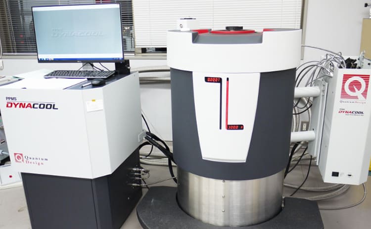
14T Magnetic and Physical Property Measurement System (Dynacool)
Dynacool is the measurement system capable of applying a high magnetic field of 14 T and temperatures from 2~1000 K. It can measure electrical properties, magnetic properties, and specific heat. Only magnetic properties measurement is available at high temperature.
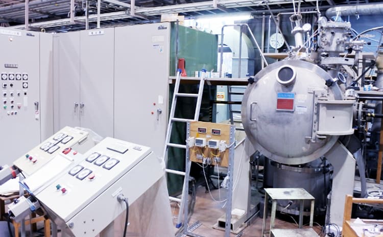
中空試験片方式 高圧水素ガス環境下材料特性評価設備群
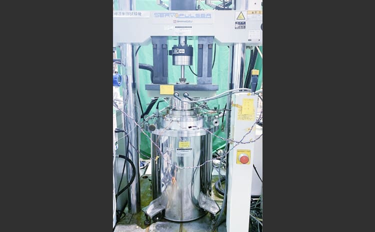
Material property test systems under high-pressure hydrogen gas environment using hollow specimens
Material property tests are conducted using hollow specimens. Slow strain rate tensile tests and fatigue tests can be performed with the hollow specimens filled with high-pressure hydrogen gas.
SEM中その場温度可変押込み試験装置
SEM Pico Indenter
Sub-micron mechanical characterization can be performed in the SEM. The measurement position can be determined with high precision, and in combination with EBSD and EDS, the microstructure-orientation-composition-mechanics relationship can be evaluated at high throughput. The measurement can be performed in a vacuum environment in the temperature range of -150℃ to 1000℃.
低温物性測定マグネット
Low Temperature Property measurement Magnets
This system can cool quantum materials down to 0.03 K and apply a magnetic field of 20 T to them. Using this system, one can study electronic properties of quantum materials such as metals, semiconductors, and superconductors.
量子デバイス電子輸送温度可変評価装置
Variable-temperature quantum transport measurement system
This system enables current-voltage measurements in the temperature range from 1.5 K to 300 K. Furthermore, a high magnetic field of up to 8 T can be applied to the sample with a superconducting magnet. The sample is fixed on an IC chip with 24 electrical lines. Therefore, the current-voltage measurement can be performed at 24 electrodes formed on the sample at the maximum.
サーモリフレクタンス法熱伝導率測定装置
Thermoreflectance method thermal conductivity measuring apparatus
Thermal conductivity can be measured not only for bulk samples but also for sample forms ranging from nano-thin films to microcrystals. Thermal conductivity of different parts of the sample can also be evaluated by site selective measurements. In addition, instead of relying on extraction trials from multiple thin film samples prepared with different thicknesses, it is possible to evaluate the interfacial thermal resistance in a single sample.
4. Sample Preparation and Synthesis (8 items)
3次元積層装置群
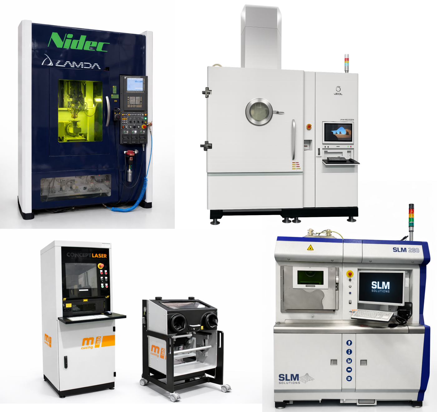
Additive Manufacturing Systems
These systems build complex metal components layer-by-layer from metal powder using high-precision lasers or electron beams. Often referred to as 3D printing, this transformative technology is redefining modern manufacturing. Our research is dedicated to achieving defect-free production while engineering next-generation materials specifically optimized for these processes.
水冷銅ルツボ高周波誘導溶解設備
Cold crucible levitation melting furnace
The amount dissolved is 1.2 kg in terms of titanium. This is a dual power source type high frequency induction melting furnace that concentrates the buoyancy and heating roles of 150 kW and 100 kW. Features: 1. Rapid dissolution possible. 2. High purity and high melting point metals can be melted. 3. Alloy melting with uniform composition. 4.Free selection of flux is possible. 5. Promote refining reactions by actively stirring the molten metal using electromagnetic force.
可視光トポロジカルレーザー作製用 GaN系物質成長装置
MOVPE system for the fabrication of GaN-based visible light topological laser
The blue LEDs changed the world's lights and won a Nobel Prize. This equipment is a highly versatile crystal growth system for nitrides. We can fabricate optical devices (UV-LED, UV-LD, PD) and electronic devices (high electron mobility transistors).
スマートラボ (全自動成膜クラスター装置)
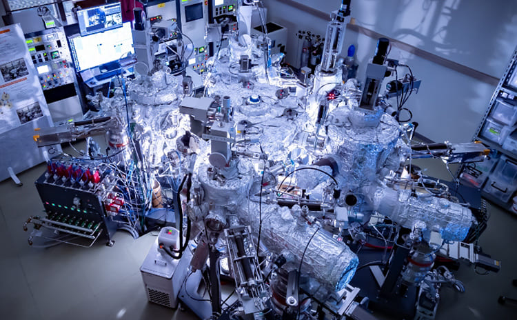
Smart Lab (fully automated cluster film deposition system)
This is a fully automated, computer-controlled film deposition system capable of fabricating samples with complex thin film multilayer structures. Automated transfer robot is used to move between sputter deposition, electron beam deposition, and molecular beam epitaxy chambers, allowing the system to be used for a wide range of fundamental thin film research.
高周波誘導熱プラズマ装置
RF induction thermal plasma system
Thermal plasma is generated and the thermal and chemical reaction zone at very high temperatures can be utilized to process inorganic materials into spherical particles. Sub-millimetre particles can be produced by ensuring sufficient droplet flight distance. It can also be applied to high-melting-point, brittle intermetallic compounds which are difficult to spheronise using conventional atomizers.
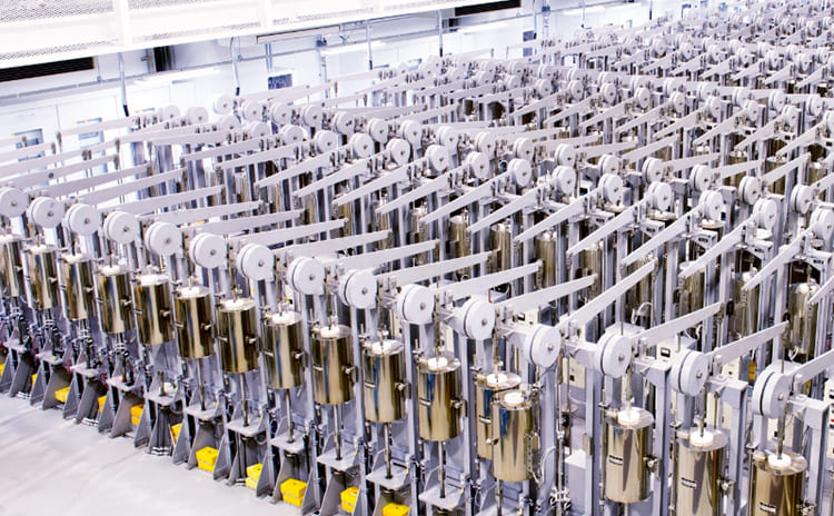
3万トンベルト型高圧装置
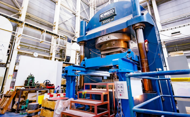
30,000-ton Belt-type high pressure apparatus
n materials synthesis research under ultrahigh pressure, a large-capacity high-pressure apparatus is required that can stably grow single crystals, etc. for long periods of time. This belt-type high-pressure apparatus mass-produces hexagonal boron nitride single crystals, which are essential for the two-dimensional atomic devices, and is provided to more than 350 research groups in 35 countries.
衝撃圧縮装置
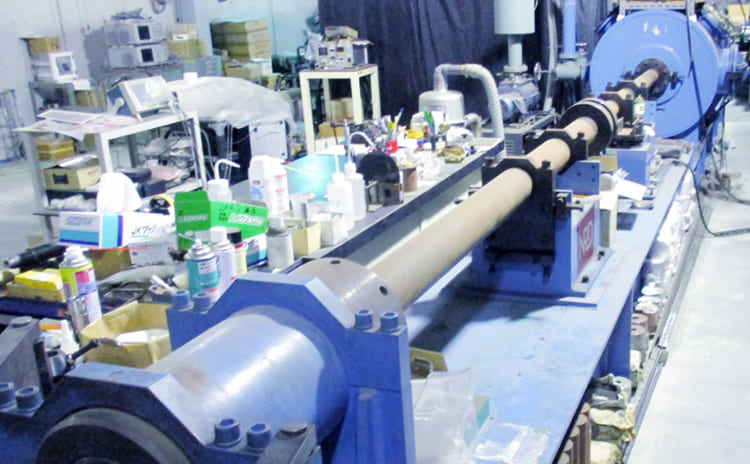
Single-stage propellant gun
This propellant gun is capable of accelerating and impacting a flying object (30 mmφ x 45 mmL) to a velocity of approximately 2 km/s and generating an impact pressure of up to about 50 GPa for approximately one-millionth of a second. This apparatus can realize characteristic high-pressure environments not only for high-pressure material synthesis, but also for meteorite impact simulation in planetary science.
HVPE成膜装置
HVPE equipment
HVPE (halide vapor phase epitaxy) equipment for gallium oxide, an ultra-wide bandgap semiconductor promising for future power device applications. Ultra-fast growth of high-quality films is possible owing to the original reactor design and chemical reaction control.
5. Materials Forming and Machining (2 items)
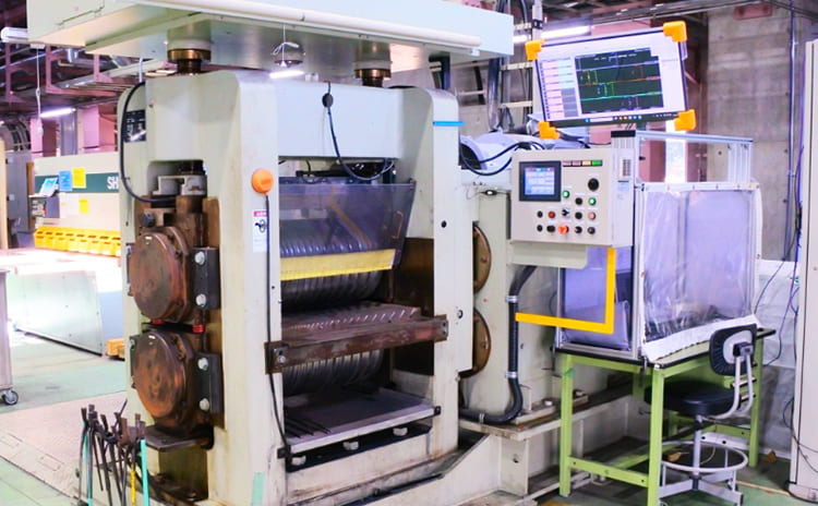
1500t鍛造シミュレータ
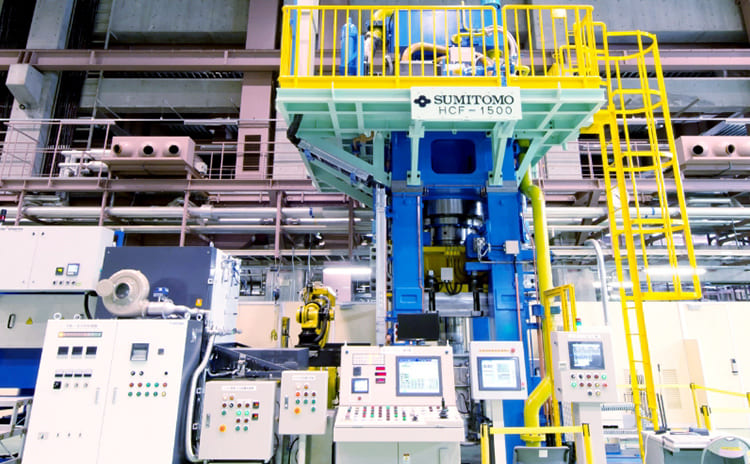
1500 ton Forging Simulator
The 1500 ton Forging Simulator apparatus enables us to precisely control the forging process parameters, such as stroke/strain rate, stress, forging temperature, heating, and cooling rate. Data obtained using this 1500 ton forging simulator are useful to analyze the effects of forging parameters on the microstructure and the mechanical properties of forged products.
歪み速度制御圧延機
Strain Rate Control Rolling Mill
This Strain Rate Control Rolling Mill allows stepless control of rolling speed from 1 to 30 m/min. Grooves range from ◇40mm to ◇7.9mm. It is capable of measuring rolling speed, load, sample temperature before and after rolling with a monochromatic radiation thermometer, and torque values. It is also equipped with a high-torque motor, and is widely used for the preparation of bar samples.
6. Material Design Support (1 item)
材料数値シミュレータ
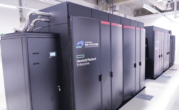
Numerical Materials Simulator
of the Japan's foremost supercomputers. It has 1,116 computational nodes and the theoretical peak performance of 4.97 PFLOPS.We always offer the architecture and the support by the NIMS engineers, which gives an advantage to new materials research in NIMS. It has contributed to producing superior world-leading outcomes by way of the theoretical calculations in the wide range of the field of materials research.
7. Facility (6 items)
微細加工クリーンルーム
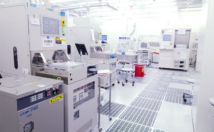
Nanofabrication Cleanroom
anofabrication cleanroom for device process research, mainly for semiconductor materials. It can be used for trials using a wide variety of materials and is suitable for everything from small samples to wafer substrates, making it suitable not only for basic fundamental research, but also for developmental R&D with an eye toward application.
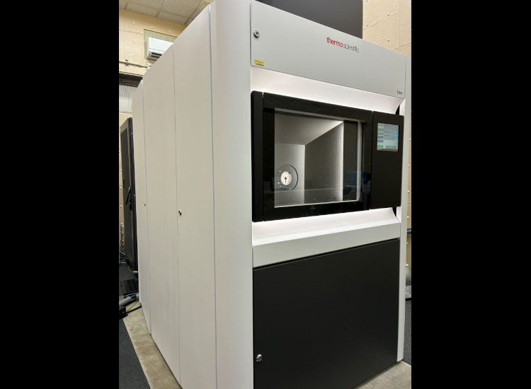
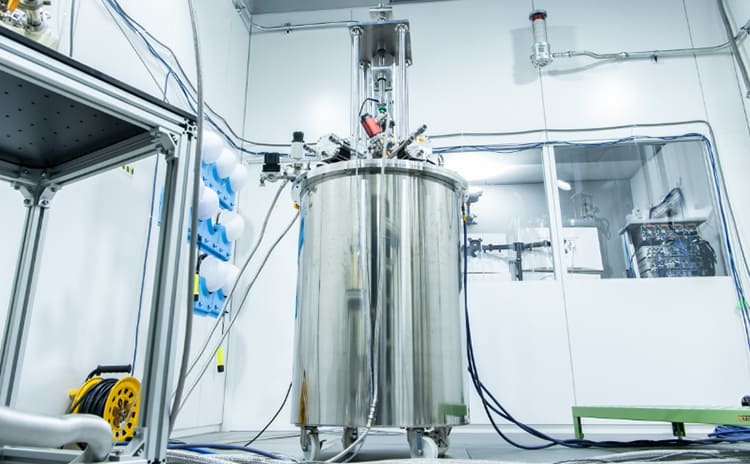
スーパードライルーム
Super-Dry Room
This super dry room boasts the world's highest level of accuracy. With an air supply dew point of -90℃ or lower and a very low moisture content of only 0.1 ppm or less, the room can be used for a wide range of applications from small battery prototyping to battery evaluation and analytical evaluation. The room provides a non-aqueous environment ideal for the development and analysis of next-generation storage batteries.
スマートラボ (単結晶X線構造解析装置)

Smart Lab (Single Crystal X-ray Diffractometer)
It is a single crystal X-ray diffractometer with an auto sample changer. 48 samples are stored in the sample container. The sample capillary in the container is auto mounted to the diffractometer by a robot arm and auto sample position adjustment to the X-ray center is carried out. XRD data of many samples are obtained by continuous unattended operation and they lead to discovery of new materials.
バイオ分析・評価エリア

Bio-related research Facilities
The facilities include a variety of equipment to support bio-related experiments. The equipment in the photo is Micro X-ray CT Imaging System in the facilities. Various types of specimens, such as small laboratory animals and organs, can be photographed, and high-resolution data can be obtained and analyzed noninvasively and over time with as little exposure as possible. The device itself is shielded, so there is no risk of radiation exposure to the operator.
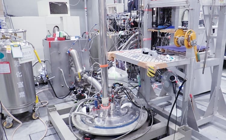
水素関連 : 水素液化磁気冷凍機
Magnetic refrigerator for hydrogen liquefaction
This refrigerator cools and liquefies hydrogen using the magnetocaloric effect, in which temperature of magnetic materials changes with changes in surrounding magnetic field. By moving magnetic materials in and out of the magnetic field applied by a superconducting magnet, the heat of the electromagnet due to change in the magnetic field is reduced and highly efficient hydrogen liquefaction is realized.
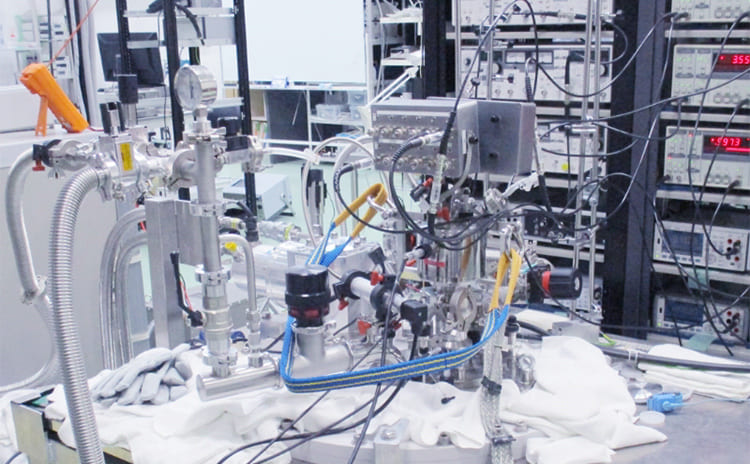
水素関連 : 水素製造装置
Hydrogen Production Machine
This is a concept-demonstrating system that produces high-purity hydrogen gas (99.9999% and above) in large quantities (100 liters per hour) from hydrocarbon gas and carbon dioxide gas. It is utilized in the research and development of advanced catalyst materials and reaction systems, aiming for the practical implementation of 'clean hydrogen' that involves no atmospheric discharge of carbon dioxide during production.