Development of a Thick-Film Conductive Ink Suitable for Large-Area, Large-Current Printed Electronics
2024.01.15
NIMS (National Institute for Materials Science)
Sumitomo Metal Mining Co., Ltd.
N.E. CHEMCAT CORPORATION
Priways Co., Ltd.
NIMS, Sumitomo Metal Mining Co., Ltd., N.E. CHEMCAT CORPORATION and Priways Co., Ltd. have jointly developed a thick-film, electrically conductive ink suitable for printing electronic circuits and sensors on the surfaces of films and other substrates to manufacture printed electronics. Sumitomo Metal Mining and Priways displayed the ink during the 38th Nepcon Japan exhibition to be held from January 24th to 26th, 2024.
Abstract
- NIMS, Sumitomo Metal Mining Co., Ltd. (based in Minato City, Tokyo), N.E. CHEMCAT CORPORATION (based in Minato City, Tokyo) and Priways Co., Ltd. (a NIMS-founded startup based in Tsukuba, Ibaraki) have jointly developed a thick-film, electrically conductive ink suitable for printing electronic circuits and sensors on the surfaces of films and other substrates to manufacture printed electronics. Sumitomo Metal Mining and Priways displayed the ink during the 38th Nepcon Japan exhibition to be held from January 24th to 26th, 2024.
- Printed electronics are manufactured using additive methods (i.e., electronic circuits are directly printed on the surfaces of substrates) rather than conventional subtractive electronics manufacturing (i.e., metallic films are first deposited on substrate surfaces and unnecessary film regions are then removed to form circuits). The additive method uses less amount of metallic materials than the subtractive method, making it more environmentally friendly and inexpensive. In addition, the additive method can be used to print electronic circuits on the surfaces not only of rigid substrates but also flexible ones. Because of these advantages, the additive method is expected to serve as an effective wiring technique for use in next-generation device fabrication.
- The new thick-film conductive ink was created using metal complex inks (i.e., inks consisting of a central metallic ion surrounded by charged molecular ligands) developed by NIMS and Priways and metallic powder synthesis and paste production technologies developed by Sumitomo Metal Mining. This ink is able to meet printed electronics requirements: its thickness is controllable and it is compatible with low-temperature sintering. These improvements were achieved by adding copper particles developed by Sumitomo Metal Mining to the ink, enabling it to form thick-film wiring at around 200°C on the surfaces of heat-resistant plastic films.
- The newly developed ink is more inexpensive to synthesize and more oxidation-resistant than conventional conductive inks. In addition, the thickness of the ink film can be more than three times larger than that of conventional ink films, making it suitable for use in large-current, large-area electronic products. The research team is currently developing techniques for mass-producing this ink by leveraging N.E. CHEMCAT’s expertise in metal complex development and production. The team plans to further improve the performance of the ink and identify other applications for it.
- This project was carried out by a research team consisting of Takeo Minari (Group Leader, Research Center for Macromolecules and Biomaterials (RCMB), NIMS), Wanli Li (Postdoctoral Researcher, RCMB, NIMS; currently Associate Professor, Jiangnan University), Lingying Li (Research Fellow, International Center for Young Scientists, NIMS), Shunto Arai (Independent Scientist, RCMB, NIMS), Chisato Niikura (Senior Researcher, RCMB, NIMS), Sumitomo Metal Mining Co., Ltd., N.E. CHEMCAT Corporation and Priways Co., Ltd.
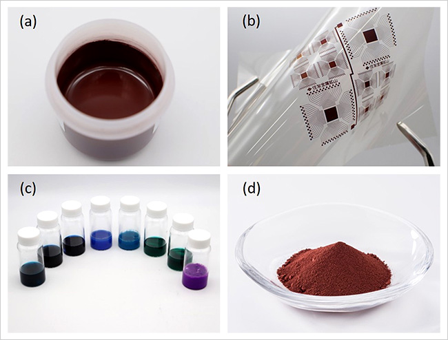
Figure. (a) Thick-film conductive ink. (b) Flexible substrate with patterns printed on its surface using the thick-film conductive ink. (c) Variety of metal complex inks that are used to synthesize the thick-film conductive ink. (d) Copper particles.
Published Paper
Contact information
(Regarding this research)
Group Leader
Printed Electronics Group
Macromolecules Field
Research Center for Macromolecules and Biomaterials, NIMS
E-mail: MINARI.Takeo=nims.go.jp (Please change "=" to "@")
(Regarding sample provision and sales)
Sumitomo Metal Mining Co., Ltd.
(General information and Media contact)
FAX: +81-29-859-2017
E-Mail: pressrelease=ml.nims.go.jp (Please change "=" to "@")
Sumitomo Metal Mining Co., Ltd.
N.E. CHEMCAT CORPORATION
Same Keywords
-
Cupric Oxide Exhibiting Both Magnetic and Dielectric Properties at Room Temperature
(copper)
2022.11.17
-
Development of an Oxidation-Resistant Copper Core–Nickel Shell Ink
(printed electronics,flexible electronics,metal complex ink,Priways)
2022.02.22
-
Development of Ultra-High-Resolution Printed Electronics Using Dual Surface Architectonics
(printed electronics,flexible electronics,Priways)
2021.05.27