

Low-Resistance Buffer Layer That Paves the Way for Vertical GaN Devices on Silicon
— Achieving Both GaN Epitaxial Growth and Vertical Electric Conduction —2026.06.15
NIMS (National Institute for Materials Science)
NIMS succeeded in developing a technique to form a GaN epitaxial film with extremely low resistance and robust thermal stability, which is essential for realizing vertical gallium nitride (GaN) devices on low-cost silicon (Si) wafers. This novel technique, an “amorphous-like interlayer (AL-IL)” approach, uses an ultrathin film composed of Si and nitrogen (N) to accommodate lattice mismatch between Si and GaN, and enables vertical current flow between the substrate and the GaN film. This achievement constitutes a fundamental technology for fabricating vertical GaN devices on Si wafers, and is expected to contribute to reducing the cost of high-efficiency power devices and micro-LED devices in the future. This research result was published in Advanced Physics Research on May 29, 2026.
Background
Key Findings
As shown in Figure 1, this technique forms an ultra-thin amorphous-like interlayer (AL-IL) containing Si and N by forming a metal film with a thickness less than 1 nanometer (one-billionth of a meter) on a Si wafer, rapidly heating it, and then depositing GaN by sputtering. The team confirmed through transmission electron microscopy observation and other means that this intermediate layer accommodates the lattice mismatch between Si and GaN and enables the epitaxial growth of GaN. The team further demonstrated that a high-quality GaN film can be grown by depositing GaN by metalorganic chemical vapor deposition (MOCVD) using a sputtered GaN film as the platform. When current-voltage (I-V) characteristics were evaluated by forming electrodes between the GaN film and the Si substrate, it was found that the electric current flows in the vertical direction (the direction of the yellow arrow in the right diagram in Figure), exhibiting ideal current characteristics for device fabrication. This achievement fulfills one of the key requirements for realizing vertical GaN devices on Si wafers.
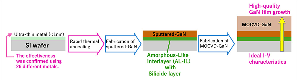
Figure. Illustration of the epitaxial growth of a GaN film on Si (111) via an amorphous-like interlayer (AL-IL)
Future Outlook
Other Information
- This project was conducted as part of “Basic research for the realization of vertical GaN devices “ led by Fumio Kawamura (Principal Researcher, Ultra-wide Bandgap Semiconductors Group, Research Center for Electronic and Optical Materials, NIMS) and Kazutaka Mitsuishi (Deputy Director, Center for Basic Research on Materials, NIMS) under the Program of the Acquisition, Technology and Logistics Agency.
- This research result was published in Advanced Physics Research (open access) on May 29, 2026.
Published Paper
Authors : Fumio Kawamura, Takeyoshi Onuma, Kazutaka Mitsuishi
Journal : Advanced Physics Research
DOI : 10.1002/apxr.70143
Publication Date : May 29, 2026


Contact information
Regarding This Research
Principal Researcher
Ultra-wide Bandgap Semiconductors Group
Research Center for Electronic and Optical Materials
National Institute for Materials Science
TEL: +81-29-860-4428
URL: https://www.nims.go.jp/electr-opt/UWBG_e.html (Ultra-wide Bandgap Semiconductors Group)
Media Inquiries
Division of International Collaborations and Public Relations
National Institute for Materials Science
1-2-1 Sengen, Tsukuba, Ibaraki 305-0047, Japan
TEL: +81-29-859-2026
FAX: +81-29-859-2017