

In our research into semiconductor diamond CVD, we are focusing on n-type doping in particular, and developing technology for controlling materials to suit the specific specifications of various devices, with the aim of forming “usable” semiconductor devices.
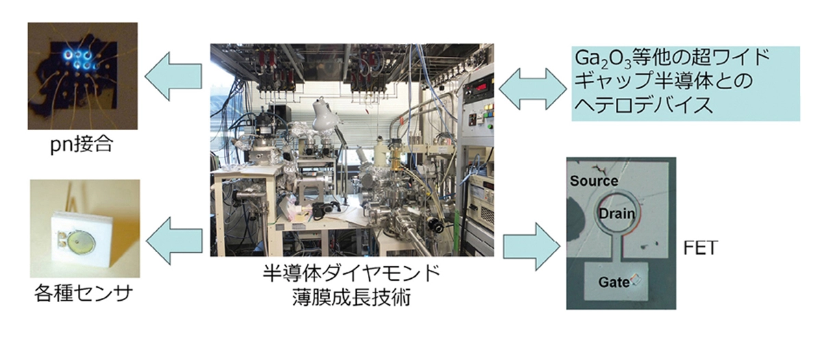
In addition, based on the knowledge gained through CVD technology, we are also conducting crystal evaluations at the device level. Hetero devices with Ga2O3, etc. are also an important research subject. We are considering applications to power electronics, sensors and semiconductor circuits used in extreme environments.
Ultra-wide Bandgap Semiconductors Group | Research Center for Electronic and Optical Materials
Ultra-wide Bandgap Semiconductors Group
Group leader
Group members
AIM and GOAL
Reducing electricity consumption is an urgent issue in order to realize a carbon-neutral society. Improving the efficiency of power semiconductor devices is an extremely effective means of saving energy.
Currently, most power semiconductor devices are made using silicon, but its performance is approaching the material limit. The use of wide bandgap semiconductors holds promise for further performance improvements, and power semiconductor devices made using SiC and GaN are becoming more widespread.
We are working on research and development of ultra-wide bandgap materials in order to contribute to the realization of high-efficiency/high-voltage power semiconductor devices and environmentally resistant devices of ultimate semiconducting characteristics.
APPROACH
Ultra-wide bandgap semiconductor materials have great potential for use in high-performance power semiconductor devices. However, many technical challenges related to crystalline defects, doping and device fabrication issues must be overcome in order to realize the ultimate semiconducting devices.
We aim to establish epitaxial growth technology and interface control technology that can contribute to solving these technical issues. For the time being, we will focus on diamond and gallium oxide, and will also actively take on newer targets.
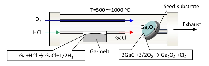
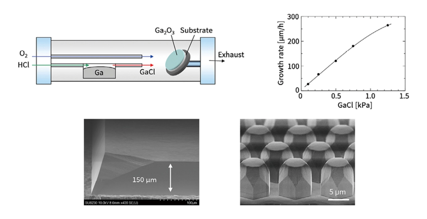
FIG 1 Ultra-high-speed, high-purity growth of Gallium Oxide using HVPE (halide vapor phase epitaxy).
» A chemical reaction with a small equilibrium constant prevents parasitic reactions, enabling film formation more than 100 times faster and with higher purity than MOCVD, etc.
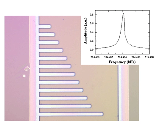
FIG 2 Achieving the world's highest quality factor with diamond MEMS resonators.
» Can be used for ultimate performance sensors (mass, acceleration, magnetism)
KOIZUMI, Satoshi / Group Leader
Diamond Semiconductor Research
Overview
Diamond is a wide-gap semiconductor material that is expected to be applied to deep-ultraviolet optoelectronics, power devices, and more.
The NIMS Diamond Research Group established diamond vapor growth technology in the 1980s and n-type semiconductor technology in the 1990s, and has succeeded in forming pn junctions in the 21st century. All of these technologies are world-firsts, and are global research achievements that Japan can be proud of.
Currently, these research projects are continuing and developing as an important part of NIMS's research into ultra-wide-bandgap semiconductors.
Characteristics
Diamond's large band gap of 5.5 eV and the unique property of its surface, the negative electron affinity, have the potential to produce a variety of devices with unique characteristics. Applications that take advantage of this property have been difficult due to imperfect doping and growth control.
We aim to develop technology for controlling impurities and crystal perfection to the level of silicon semiconductors, thereby realizing usable diamond materials.
Major reserch
Summary
- Successfully fabricating various diamond devices through advanced n-type doping
- Exploring diamond vapor phase growth technology as the ultimate power device semiconductor material
- Peer-reviewed papers: 186, patents granted: 7
LIAO, Meiyong
Diamond MEMS, Electronic, and Optical Devices and Systems
Overview
Diamond is the ultimate semiconductor material, possessing physical properties that far exceed those of currently used semiconductors. It is expected to deliver unparalleled performance in applications for microelectromechanical systems (MEMS) and electronic devices.
Diamond is the most promising semiconductor candidate for highly sensitive and reliable MEMS sensors (for magnetic fields, temperature, vibration, acceleration, etc.), high-frequency mechanical oscillators, and electronic devices capable of withstanding extreme conditions, including high voltage, high temperature and high radiation that existing semiconductor materials cannot endure.
Our research focuses on the development of high-quality diamond wafers through CVD growth, as well as the advancement of MEMS devices, optical and electronic devices and their systems.
Characteristics
- Leadership in smart-cut single-crystal diamond MEMS technologies
- Development of ultrahigh-quality factor and high-reliability MEMS resonators
- Innovation in diamond MEMS sensing chip
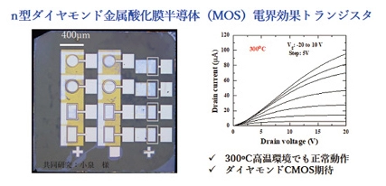
- Demonstration of n-channel diamond transistors
Major reserch
We have achieved a number of cutting-edge research breakthroughs, including batch manufacturing of single-crystal diamond MEMS, the highest-temperature MEMS magnetic sensors, actuators, and diamond transistors.
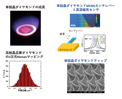
- We developed the smart-cut method for diamond cantilevers with a record-high quality factor (Q > 1,000,000) at room temperature and theoretically demonstrated the superiority of diamond MEMS by elucidating its mechanical energy loss mechanisms.
- We developed a universal single-crystal diamond MEMS chip, which exhibited outstanding properties, including high sensitivity, low operating voltage, and high-temperature operation (600℃).
- We developed a diamond MEMS magnetic sensor and sensor array capable of operating at high temperatures (500℃) while maintaining high magnetic sensitivity (10nT/Hz0.5).
- These achievements are expected to enable applications for wear-resistant scanning probe microscopy, high-precision temperature sensing in microscale, internal combustion engines control, petroleum and mineral exploration. Furthermore, we realized the n-channel diamond MOSFETs, paving the way for the development of diamond CMOS.
Summary
We developed the smart-cut method that is highly reproducible and well-controlled for diamond MEMS (i.e. cantilevers, bridges, membranes). The developed diamond MEMS sensors have been proven to possess significantly higher reliability and sensitivity compared to other semiconductor materials. Microscale high-precision and high-reliability sensor arrays (magnetic, temperature, light, etc) that the existing ones cannot reach are under development.
OSHIMA, Yuichi
Development of high-speed, high-quality epitaxial growth technology for ultra-wide-gap semiconductors
Overview
To realize energy conservation for a decarbonized society, development of low-loss power devices is an urgent issue. Currently, most power semiconductor devices are made using Si, but their performance is close to the material limit. Therefore, there is a need to realize and popularize ultra-wide bandgap (UWBG) semiconductor power devices with higher performance than that of Si.
In this study, we aim to establish high-quality and high-speed epitaxial growth technologies necessary to extract the excellent potential of such new materials and to fabricate high-performance devices with sufficient cost effectiveness.
Characteristics
- Application of halide vapor phase epitaxy (HVPE) for UWBG materials
- Much higher growth rate than that of MOCVD, etc. by effectively preventing parasitic reaction.
- High purity crystal growth technology that contributes to good control of electrical properties
- Defect density reduction technology that makes full use of growth mode control and selective growth
Major reserch
We are aiming to establish the HVPE method, which has a proven track record in high-speed deposition of III-V compound semiconductors such as GaN, for the growth of Ga2O3, which is attracting attention as a UWBG semiconductor.
So far, we have achieved ultrahigh-speed growth of over 100 µm/h through our unique reactor design and parasitic reaction suppression technology by optimizing the balance between growth and etching reactions, and have succeeded in growing thick films of over 100 µm using this method. We also succeeded in achieving both selective area growth and high-speed growth, and succeeded in significantly reducing dislocation density.
These results will greatly contribute to the realization of high-voltage Ga2O3 power devices with thick drift layers exceeding several tens of µm.
Summary
We have demonstrated ultrafast thick film growth of Ga2O3, which is attracting attention as a next-generation high-performance power device material, by HVPE method and defect reduction by selective area growth.
The technique for high-speed growth with suppression of parasitic reactions even in the case of precipitation reactions with large equilibrium constants, obtained in this study, is expected to be applicable to new material systems other than Ga2O3.
OSHIMA, Takayoshi
New structural control of oxide power semiconductors
Overview
To achieve carbon neutrality, the semiconductor industry requires the practical implementation of next-generation power semiconductors that enable ultra-low-loss power devices. Among these materials, Ga₂O₃ and rutile-type oxides (such as SnO₂ and GeO₂) have a relatively short research history. However, compared to more established materials like SiC and GaN, these oxide semiconductors exhibit superior fundamental properties for power device applications and have recently attracted increasing attention.
In this study, we employ selective area growth and selective gas etching techniques on these relatively new oxide power semiconductors to promote facet formation, enabling structural control essential for enhancing device performance.
Characteristics
- Plasma-free microfabrication technology
- High-aspect-ratio structures that cannot be fabricated using conventional techniques
- Device fabrication utilizing plasma-damage-free and high-aspect-ratio structures
Major reserch
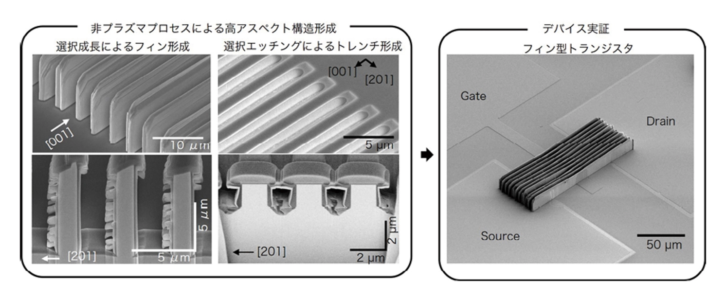
As an example of this study, we explain the plasma-free microfabrication of Ga2O3 semiconductors.
This semiconductor is n-type unipolar, and thus it is unable to form a pn homojunction. Therefore, to enhance the performance of unipolar devices, it is necessary to control the electric field in microscopic regions using high-aspect-ratio structures such as fins and trenches. In conventional microfabrication, plasma-based dry etching is commonly used. However, this approach has limitations, including the difficulty of forming high-aspect-ratio structures and the introduction of processing damage to the surface due to reactive ions.
In this study, we demonstrated selective growth and selective gas etching as new processing methods capable of overcoming these challenges. These techniques expose chemically stable faceted sidewalls, enabling the fabrication of fin and trench structures, as shown in the figure, without the use of reactive ions.
Currently, we have also attempted fabricating devices that utilize these fin and trench structures.
Summary
By utilizing crystallographic growth and etching microfabrication techniques, it becomes possible to fabricate high-aspect-ratio structures that were previously difficult to fabricate using conventional techniques. We will verify the effectiveness of this method through device fabrication and evaluation. Additionally, we plan to extend this research beyond Ga₂O₃ to recently proposed rutile-type oxide power semiconductors.
IROKAWA, Yoshihiro
Characterization of semiconductor devices
Overview
Reliability of semiconductor devices is a critical issue. For example, ambient atmosphere is known to alter the device characteristics, but the fundamental mechanism of the phenomenon is still unclear.
In this research, the effects of ambient atmosphere on nitride-based semiconductor devices are investigated.
Characteristics
Proposal of the physical model and development of hydrogen sensors
Major reserch
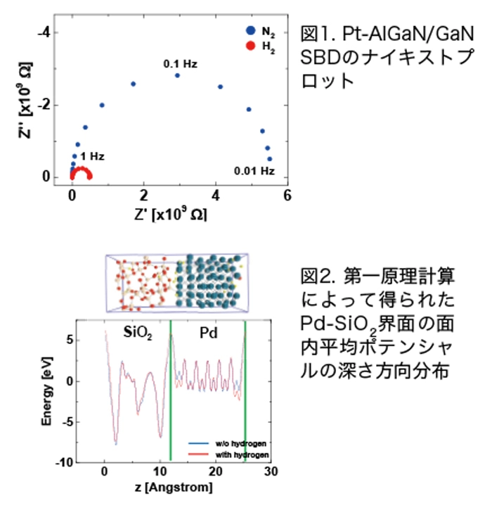
We investigated the metal/semiconductor interfaces. Figure 1 shows Nyquist plots of Pt-AlGaN/GaN SBDs. As shown in Fig. 1, a new semi-circle representing electric double layers are not confirmed. Figure 2 shows the calculated average potential at Pd-SiO2 interfaces. As shown in Fig. 2, the average potential at Pd-SiO2 interfaces does not changed after hydrogen introduction.
Based on these results, formally proposed hydrogen induced dipole model would not be the responsible mechanism. Through vigorous study, we have confirmed that dielectric layers at metal/semiconductor interfaces play a critical role.
Summary
Obtained results would be applicable not only to contributing to the reliability of semiconductor devices but also to the improvement of hydrogen sensors.
KAWAMURA, Fumio
Development of novel thin-film and bulk materials via high-pressure techniques.
Overview
A belt-type high-pressure apparatus enables us to achieve pressures and temperatures of up to 8 GPa and 2400 ℃ when synthesizing functional thin films and bulk materials. In particular, the combination of metathesis reaction and high-pressure synthesis makes it possible to create a wide variety of new materials, including nitride semiconductors, ultra-hard materials, superconducting materials, and so on. Very recently, we have begun to explore the synthesis of highly functional thin-film materials by utilizing large-volume high-pressure cells.
Characteristics
Conventionally, the development of new materials under high pressure has been attempted by utilizing phase transitions from atmospheric pressure phases to high-pressure phases. In this case, the necessity of preparation of ordinary pressure phases restricts the variety of materials produced under high-pressure.
Our research theme, "chemical reactions under high pressure (particularly metathesis reactions)," which is currently under development, will make it possible to create a variety of new substances, eliminating the need to prepare an atmospheric pressure phase for phase transition.
Major reserch
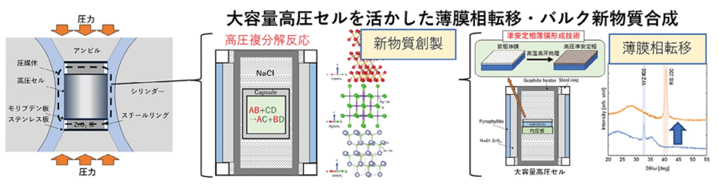
The left figure shows a conceptual diagram of a belt-type high-pressure apparatus. The high-pressure cell is pressurized using a cemented carbide anvil, and then electricity is applied to achieve high temperature and pressure. The middle figure denotes a schematic diagram of the setup for chemical reactions in a high-pressure cell. For example, by mixing halides and alkaline earth metal nitrides as reagents, a strong nitriding reaction occurs, and various novel nitrides are synthesized. So far, novel materials such as the layered superconducting material ReN2, new superhard materials W3N4, novel nitride semiconductors MgSnN2 and CaSnN2 and so on have been synthesized.
We are also working on thin film technology to develop these materials into devices in the future. The figure on the right shows an example of the application of MgSnN2, a new semiconductor bulk-synthesized under high pressure, as a thin-film material using the sputtering method. The MgSnN2 thin film with a high-pressure phase was successfully obtained by applying high temperature and pressure to a thin-film precursor that had been fabricated on the substrate.
The technique of processing thin films at high temperatures and high pressures is expected to cause an innovation such as converting semiconductor materials that could previously be synthesized as only n-type to p-type.
Summary
With ongoing advancements of high-temperature and pressure synthesis techniques, we will commit to the development of novel materials through the application of high-pressure annealing technology to thin films, with the purpose of enabling innovative device fabrication.
SASAMA, Yosuke
Diamond electronic devices
Overview
Diamond is a wide-gap semiconductor that possesses exceptional properties surpassing conventional semiconductor materials, including high carrier mobility, high breakdown electric field, and high thermal conductivity. I am developing next-generation electronic devices by harnessing the outstanding semiconductor properties of diamond. For instance, the utilization of diamond in power devices could reduce power losses during power conversion, potentially contributing to the achievement of a decarbonized and sustainable society.
Characteristics
- Fabricated diamond field-effect transistors (FETs) featuring high-quality hydrogen-terminated diamond/hexagonal boron nitride (h-BN) heterostructures
- Achieved high channel mobility of ≈1000 cm2V-1s-1 in p-channel FETs based on wide-gap semiconductors
Major reserch
In my view, while diamond possesses excellent semiconductor properties, its full potential has not yet been realized in current devices. One of the challenges is the low channel mobility in diamond field-effect transistors (FETs). We have fabricated high-quality hydrogen-terminated diamond/h-BN heterostructures and achieved high mobility in diamond FETs. As a result, we have realized a high channel mobility of ≈1000 cm2V-1s-1 in wide-gap semiconductor-based p-channel FETs.
Summary
Diamond holds great promise as a next-generation semiconductor material for realizing a sustainable society. My research focuses on enhancing the performance of diamond semiconductor devices, aiming to contribute to solving societal challenges. I will continue developing innovative semiconductor devices that harness the full potential of diamond.
Current Members (as of 2026)
Postdoctoral Research Fellow
ZHANG Zhaozong ZHANG.Zhaozong@nims.go.jp
MOHAMMAD Monish MOHAMMAD.Monish@nims.go.jp
Temporary Staff(engineering)
ARAI, Nobuaki ARAI.Nobuaki@nims.go.jp
Visiting Researcher
SHIMAOKA, Takehiro SHIMAOKA.Takehiro@nims.go.jp
CHEN Guo
 CHEN.Guo@nims.go.jp

