Discovery of Topological LC Circuits Transporting EM Waves without Backscattering
— Honeycomb structure is the key, may open a new door towards miniaturization of microwave devices, including mobile phones—
2018.11.19
National Institute for Materials Sciences
NIMS succeeded in fabricating topological LC circuits arranged in a honeycomb pattern where electromagnetic (EM) waves can propagate without backscattering even when pathways turn sharply.
Abstract
- NIMS succeeded in fabricating topological LC circuits arranged in a honeycomb pattern where electromagnetic (EM) waves can propagate without backscattering even when pathways turn sharply. These circuits may be suitable for use as high-frequency electromagnetic waveguides, which would allow miniaturization and high integration in various electronics devices, such as mobile phones.
- There has been a surge in searching for materials with topological properties, whose functions are not influenced even if the sample shapes are changed. Topological properties were first discovered in electron systems, and more recently the notion has been developed for light and microwaves, which is expected to be useful for building optical and electromagnetic waveguides immune to backscattering. However, realization of topological properties in light and microwaves normally requires gyromagnetic materials under an external magnetic field, or some complex structures. In order to match existing electronics and photonics technologies, it is important to achieve topological properties based on conventional materials and simple structures.
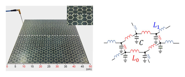
- In 2015, this research team successfully demonstrated topological properties in light and microwaves in a honeycomb lattice of dielectric cylinders, such as silicon. This time, the team revealed theoretically in a microstrip, a flat circuit, that electromagnetic waves attain topological properties when the metallic strips form a honeycomb pattern and the intra-hexagon and inter-hexagon strip widths are different. The team also fabricated microstrips and measured electric fields on their surfaces, and successfully observed the detailed structure of topological electromagnetic modes, where vortices of electromagnetic energy polarized in a specific direction are generated during the wave propagation.
- This research demonstrates that topological propagation of electromagnetic waves can be induced using conventional materials in a simple structure. Because topological electromagnetic wave propagation is immune to backscatter even when pathways turn sharply, designs of compact electromagnetic circuits become possible, leading to miniaturization and high integration of electronics devices. In addition, the direction of vortex and the vorticity associated with topological electromagnetic modes may be used as data carriers in high-density information communications. All these features may contribute to the development of advanced information society represented by IoT and autonomous vehicles.
- This project was carried out by a research team consisting of Xiao Hu (MANA Principal Investigator, International Center for Materials Nanoarchitectonics [WPI-MANA], NIMS), Toshikaze Kariyado (Researcher, WPI-MANA, NIMS) and a group led by Hong Chen (Professor, Tongji University, China).
This project was supported by the Grant-in-Aid for Scientific Research (B) “Study on mechanism of generation of topological states and creation of novel functions based on real-space manipulation.” - The paper was published in Nature Communications, an open access journal, on November 2, 2018.

Figure: Microstrip arrays (left) and LC circuit (right)
Related files
- MANA
Contacts
(Regarding this research)
-
HU Xiao
MANA Principal Investigator,
International Center for Materials Nanoarchitectonics (WPI-MANA)
National Institute for Materials Science
TEL: +81-29-860-4897
E-Mail: HU.Xiao=nims.go.jp
(Please change "=" to "@")
(For general inquiries)
-
Public Relations Office
National Institute for Materials Sciences
Tel: +81-29-859-2026
Fax: +81-29-859-2017
E-Mail: pressrelease=ml.nims.go.jp
(Please change "=" to "@")
Same Keywords
-
Fabrication of Printed High-Performance Thin-Film Transistors Operable at One Volt
(circuit)
2021.05.27
-
Development of Ultra-High-Resolution Printed Electronics Using Dual Surface Architectonics
(circuit)
2021.05.27
-
Discovery of a Mechanism for Making Superconductors More Resistant to Magnetic Fields
(topological)
2021.03.05
