Fastest Neuromorphic, Electric Double Layer Transistor
—Technology May Be Used to Develop Faster, Versatile Edge AI Devices—
2023.07.07
National Institute for Materials Science (NIMS)
Tokyo University of Science
A research team consisting of NIMS and the Tokyo University of Science has developed the fastest electric double layer transistor using a highly ion conductive ceramic thin film and a diamond thin film.
(”Ultrafast-switching of an all-solid-state electric double layer transistor with a porous yttria-stabilized zirconia proton conductor and the application to neuromorphic computing” Makoto Takayanagi, Daiki Nishioka, Takashi Tsuchiya, Masataka Imura, Yasuo Koide, Tohru Higuchi, and Kazuya Terabe; Journal: Materials Today Advances [June 16, 2023]; DOI : 10.1016/j.mtadv.2023.100393)
Abstract
- A research team consisting of NIMS and the Tokyo University of Science has developed the fastest electric double layer transistor using a highly ion conductive ceramic thin film and a diamond thin film. This transistor may be used to develop energy-efficient, high-speed edge AI devices with a wide range of applications, including future event prediction and pattern recognition/determination in images (including facial recognition), voices and odors.
- An electric double layer transistor works as a switch using electrical resistance changes caused by the charge and discharge of an electric double layer formed at the interface between the electrolyte and semiconductor. Because this transistor is able to mimic the electrical response of human cerebral neurons (i.e., acting as a neuromorphic transistor), its use in AI devices is potentially promising. However, existing electric double layer transistors are slow in switching between on and off states. The typical transition time ranges from several hundreds of microseconds to 10 milliseconds. Development of faster electric double layer transistors is therefore desirable.
- This research team developed an electric double layer transistor by depositing ceramic (yttria-stabilized porous zirconia thin film) and diamond thin films with a high degree of precision using a pulsed laser, forming an electric double layer at the ceramic/diamond interface. The zirconia thin film is able to adsorb large amounts of water into its nanopores and allow hydrogen ions from the water to readily migrate through it, enabling the electric double layer to be rapidly charged and discharged. This electric double layer effect enables the transistor to operate very quickly. The team actually measured the speed at which the transistor operates by applying pulsed voltage to it and found that it operates 8.5 times faster than existing electric double layer transistors, setting a new world record. The team also confirmed the ability of this transistor to convert input waveforms into many different output waveforms with precision—a prerequisite for transistors to be compatible with neuromorphic AI devices.
- This research project produced a new ceramic thin film technology capable of rapidly charging and discharging an electric double layer several nanometers in thickness. This is a major achievement in efforts to create practical, high-speed, energy-efficient AI-assisted devices. These devices, in combination with various sensors (e.g., smart watches, surveillance cameras and audio sensors), are expected to offer useful tools in various industries, including medicine, disaster prevention, manufacturing and security.
- This research was published in the June 16, 2023 issue of Materials Today Advances (DOI: 10.1016/j.mtadv.2023.100393).
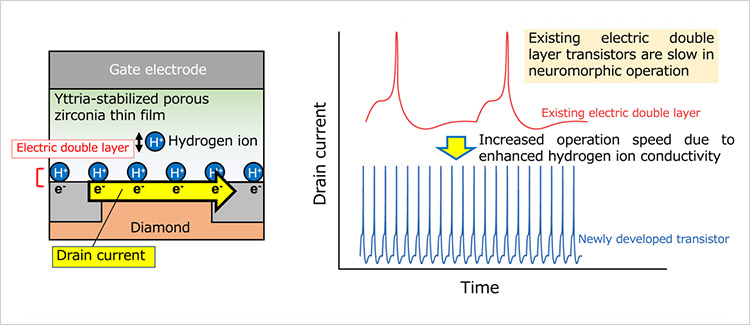
Figure. (Left) Schematic diagram of the electric double layer transistor developed in this research project. (Right) Significantly higher neuromorphic operation speed was achieved using this transistor compared to existing electric double layer transistors.
Related files
- Research Center for Materials Nanoarchitectonics (MANA)
Contact information
(Regarding this research)
-
Takashi Tsuchiya
Principal Researcher
Ionic Devices Group
Research Center for Materials Nanoarchitectonics (MANA)
National Institute for Materials Science
Tel: +81-29-860-4563
E-Mail: TSUCHIYA.Takashi=nims.go.jp
(Please change "=" to "@")
(General information)
-
Public Relations Office
National Institute for Materials Science (NIMS)
Tel: +81-29-859-2026
Fax: +81-29-859-2017
E-Mail: pressrelease=ml.nims.go.jp
(Please change "=" to "@") -
Public Relations Section
Tokyo University of Science
1-3 Kagurazaka, Shinjuku-ku, Tokyo 162-8601, Japan
Tel: +81-3-5228-8107
Fax: +81-3-3260-5823
E-Mail: koho=admin.tus.ac.jp
(Please change "=" to "@")