Alternating Triangular Charge Density Wave Domains Observed within a Layered Superconducting Compound
2024.02.26
NIMS (National Institute for Materials Science)
Tokyo University of Science
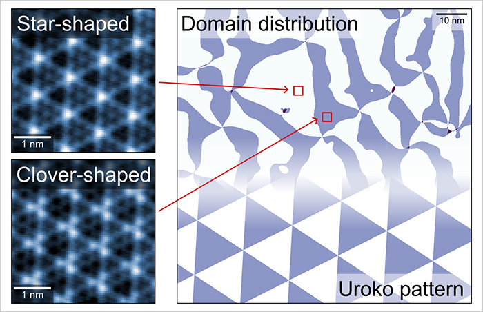
A research team consisting of NIMS and the Tokyo University of Science observed charge density waves (CDWs) within Niobium diselenide (NbSe2)—a layered compound—at cryogenic temperatures and discovered that they form alternating triangular domains characterized by two distinctive star-shaped and clover-shaped CDW structures.
Abstract
- A research team consisting of NIMS and the Tokyo University of Science observed charge density waves (CDWs) within Niobium diselenide (NbSe2)—a layered compound—at cryogenic temperatures and discovered that they form alternating triangular domains characterized by two distinctive star-shaped and clover-shaped CDW structures. This domain structure was found to be consistent with a theoretical prediction made about four decades ago.
- NbSe2—a layered superconducting compound—is often used in basic research on quantum phenomena. It is therefore important to understand the physical properties of NbSe2 in detail at cryogenic temperatures. These include the unique property it possesses to exhibit both superconductivity and CDWs (i.e., periodic modulations in electron density within the compound) and the interplay between them. Ascertaining these interactions will require the identification of a precise CDW domain structure within NbSe2. Previous research had found that CDWs within NbSe2 appeared to have two types of domains characterized by star-shaped and clover-shaped CDW structures. However, the distribution of these two domains remained undetermined due to a lack of quantitative techniques capable of accurately elucidating them.
- This research team captured high-resolution images of CDWs within NbSe2 using a scanning tunneling microscope (STM) capable of imaging crystalline surfaces with atomic-level resolution. The team then succeeded in clearly imaging the distribution patterns of the domains characterized by star-shaped and clover-shaped CDW structures by numerically determining the displacement of CDW modulations relative to the atomic lattice observed. The resulting image revealed that both domains had triangular shapes and were arranged in an alternating pattern similar to urokomon, a decorative motif resembling the scales of a fish or reptile often found in traditional Japanese art and crafts. This was the first-ever observation of the CDW domain structure since its existence was theoretically predicted in the 1980s.
- These results are expected to advance the understanding of CDWs within NbSe2 and other related compounds and facilitate high-temperature superconductor research by providing new insights into the relationship between CDWs and superconductivity. In addition, they may promote basic research on quantum phenomena in systems in which these compounds can be used as building blocks.
- This project was carried out by a research team consisting of Shunsuke Yoshizawa (Senior Researcher, Nanoprobe Group, Center for Basic Research on Materials (CBRM), NIMS), Keisuke Sagisaka (Principal Researcher, Nanoprobe Group, CBRM, NIMS) and Hideaki Sakata (Professor, Department of Physics, Tokyo University of Science).
- This research was published in the February 2, 2024 issue of Physical Review Letters (vol. 132, issue 5): https://doi.org/10.1103/PhysRevLett.132.056401.

Figure. Distribution of domains characterized by star-shaped and clover-shaped CDW structures observed within NbSe2. The domain distribution pattern somewhat resembles urokomon, a decorative motif resembling the scales of a fish or reptile often found in traditional Japanese art and crafts.
Related files
- Center for Basic Research on Materials (CBRM)
Contact information
(Regarding this research)
-
Shunsuke Yoshizawa
Senior Researcher
Nanoprobe Group
Advanced Materials Characterization Field
Center for Basic Research on Materials (CBRM), NIMS
Tel: +81-29-859-2126
E-Mail: YOSHIZAWA.Shunsuke=nims.go.jp
(Please change "=" to "@")
(General information)
-
Public Relations Office, NIMS
Tel: +81-29-859-2026
Fax: +81-29-859-2017
E-Mail: pressrelease=ml.nims.go.jp
(Please change "=" to "@") -
Public Relations Section
Tokyo University of Science
1-3 Kagurazaka, Shinjuku-ku, Tokyo 162-8601, Japan
Tel: +81-3-5228-8107
E-Mail: koho=admin.tus.ac.jp
(Please change "=" to "@")
