High-Quality Mono-Silicon Crystal Grown at Low Cost for Solar Cells
—New Casting Method May Facilitate the Return of a Market-Competitive Solar Cell Industry—
2015.10.27
(2016.01.13 Update)
National Institute for Materials Science (NIMS)
A joint NIMS and Kyushu University research team has developed a “single-seed cast method,” a new casting method making it possible to grow high-quality mono silicon at low cost.
(This study was published in the Solid State Phenomena Vol. 242 (Sep. 20, 2015): Takashi Sekiguchi, Yoshiji Miyamura, Hirofumi Harada, Karolin Jiptner, Jun Chen, Ronit R. Prakash, Satoshi Nakano, Bing Gao and Koichi Kakimoto: 50 cm size Seed Cast Si ingot growth and its characterization [DOI: 10.4028/www.scientific.net/SSP.242.30] )
Abstract
- A research team led by Takashi Sekiguchi, a leader of the Nano Device Characterization Group, Nano-Electronic Materials Unit, International Center for Materials Nanoarchitectonics (MANA), National Institute for Materials Science (NIMS), and Koichi Kakimoto, a professor at the Research Institute for Applied Mechanics, Kyushu University, has developed a new method to grow high-quality mono silicon at low cost.
- The research resulted in the invention of a new casting method called a single-seed cast method. It dramatically improved the quality of crystals created compared to conventional casting methods, which potentially leads to the development of more efficient silicon solar cells.
- As the current conversion efficiency of mainstream silicon-type solar cells has already reached 20%, it is required in future development to increase conversion efficiency even more to add higher value to the cell products. However, this goal is not achievable using conventionally cast polycrystalline silicon. In addition, there is demand for the development of a new silicon material to replace polycrystalline silicon and single-crystal silicon for semiconductors, because dislocation-free single crystal silicon for semiconductors is not adequately competitive pricewise.
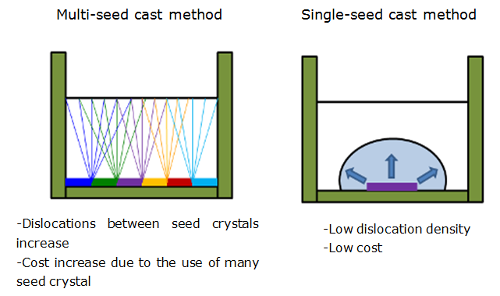
- To address this issue, the research team developed a single-seed cast method, a new silicon casting method using a seed crystal, and succeeded in growing a high-quality single-crystal silicon (mono silicon) ingot with low impurity. In the new casting method, silicon is melted in a crucible, and a single crystal is grown from a small seed crystal. This method is less expensive than the method to create single crystal silicon for semiconductors due to reduced raw material use and manufacturing costs. Moreover, the conversion efficiency of a solar cell prototype created using the crystal grown by this method was as high as 18.7%. This efficiency was very close to the efficiency of dislocation-free single-crystal silicon (Czochralski (Cz) silicon) wafers for semiconductors (18.9%), which were evaluated concurrently. In future studies, the conversion efficiency of mono silicon may exceed that of Cz silicon by further reducing crystal defects and the impact of impurities.
- It is also feasible to grow an ingot as large as a 50-cm cube using the current facility. As such, the facility is compatible with and can be integrated into the existing production line. In the future, it may be possible to make the solar cell industry market competitive again by transferring this new technology and other technologies derived from it to solar cell manufacturers in Japan.
- This research was conducted as a part of the NEDO project titled “Development of next-generation high-performance technology for photovoltaic power generation system.” This study has been published in the 9-20-2015 issue (Vol. 242) of Solid State Phenomena, and presented at the FY2015 NEDO new energy research report meeting on October 28.

Figure: Characteristics of the newly developed single-seed cast method.
Related files
- Nano-Electronics Materials Unit
Contacts
(Regarding this research)
-
Takashi Sekiguchi
Leader of the Nano Device Characterization Group,
Nano-Electronic Materials Unit, MANA, NIMS
Tel: +81-29-860-4297
E-Mail: Sekiguchi.takashi=nims.go.jp
(Please change "=" to "@")
(Regarding public relations)
-
Public Relations Office
National Institute for Materials Science
1-2-1 Sengen, Tsukuba, Ibaraki, 305-0047, JAPAN
Tel: +81-29-859-2026
Fax: +81-29-859-2017
E-Mail: pressrelease=ml.nims.go.jp
(Please change "=" to "@")
