Development of a Diamond Transistor with High Hole Mobility
—Unconventional Removal of Acceptors Enhanced Performance—
2022.01.18
National Institute for Materials Science (NIMS)
University of Tsukuba
Using a new fabrication technique, NIMS has developed a diamond field-effect transistor (FET) with high hole mobility, which allows reduced conduction loss and higher operational speed.
Abstract
- Using a new fabrication technique, NIMS has developed a diamond field-effect transistor (FET) with high hole mobility, which allows reduced conduction loss and higher operational speed. This new FET also exhibits normally-off behavior (i.e., electric current flow through the transistor ceases when no gate voltage is applied, a feature that makes electronic devices safer). These results may facilitate the development of low-loss power conversion and high-speed communications devices.
- Diamond has excellent wide bandgap semiconductor properties: its bandgap is larger than those of silicon carbide and gallium nitride, which are already in practical use. Diamond therefore could potentially be used to create power electronics and communications devices capable of operating more energy efficiently at higher speeds, voltages and temperatures. A number of R&D projects have previously been carried out with the aim of creating FETs using hydrogen-terminated diamonds (i.e., diamonds with their superficial carbon atoms covalently bonded with hydrogen atoms). However, these efforts have failed to fully exploit diamonds’ excellent wide bandgap semiconductor properties: the hole mobility (a measure of how quickly holes can move) of these diamond-integrated transistors was only 1–10% that of the diamonds before integration.
- The NIMS research team succeeded in developing a high-performance FET by using hexagonal boron nitride (h-BN) as a gate insulator instead of conventionally used oxides (e.g., alumina), and by employing a new fabrication technique capable of preventing the surface of hydrogen-terminated diamond from being exposed to air. At high hole densities, the hole mobility of this FET was five times that of conventional FETs with oxide gate insulators. FETs with high hole mobility can operate with lower electrical resistance, thereby reducing conduction loss, and can be used to develop higher speed and smaller electronic devices. The team also demonstrated normally-off operation of the FET, an important feature for power electronics applications. The new fabrication technique enabled removal of electron acceptors from the surface of the hydrogen-terminated diamond. This was the key to the team’s success in developing the high-performance FET, although these acceptors had generally been thought to be necessary in inducing electrical conductivity in hydrogen-terminated diamonds.
- These results are new mileposts in the development of efficient diamond transistors for high-performance power electronics and communications devices. The team hopes to further improve the physical properties of the diamond FET and to make it more suitable for practical use.
- This project was carried out by NIMS researchers (Yosuke Sasama, Taisuke Kageura, Masataka Imura, Kenji Watanabe, Takashi Taniguchi, Takashi Uchihashi and Takahide Yamaguchi (also an associate professor at University of Tsukuba)). This study was conducted in conjunction with other projects, including the one entitled “Creation of a high-mobility field-effect transistor with a heterostructure of diamond and hexagonal boron nitride and exploration of quantum transport in it” (project number: 19H02605) funded by the JSPS Grant-in-Aid for Scientific Research (B).
- This research was published in Nature Electronics, an online journal, on December 23, 2021 (https://doi.org/10.1038/s41928-021-00689-4).
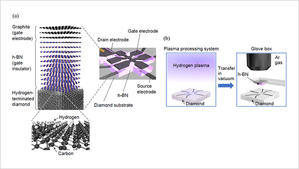
Figure. (a) Structure of the diamond field-effect transistor (FET) fabricated in this research. The design of this FET allows Hall measurements to be performed while applying a gate voltage, enabling evaluation of the density and mobility of holes in the FET channel. (b) The surface of the diamond substrate was first exposed to hydrogen plasma to terminate it with hydrogen. The substrate was then transferred in vacuum into a glovebox filled with argon gas. Finally, cleaved single-crystalline hexagonal boron nitride (h-BN) was attached to the diamond substrate, thereby reducing the amount of airborne substance—which act as acceptors—attaching to the diamond surface.
Related files
- International Center for Materials Nanoarchitectonics (MANA)
Contact information
(Regarding this research)
-
Takahide Yamaguchi
Principle Researcher,
Surface Quantum Phase Materials Group
International Center for Materials Nanoarchitectonics
Tel:+81-29-860-4885
E-Mail: YAMAGUCHI.Takahide=nims.go.jp
(Please change "=" to "@")
(General information)
-
Public Relations Office
National Institute for Materials Science
Tel: +81-29-859-2026
Fax: +81-29-859-2017
E-Mail: pressrelease=ml.nims.go.jp
(Please change "=" to "@")
Same Keywords
-
Breakthrough Iron-Based Magnetic Material Achieves Major Reduction in Core Loss
(power electronics)
2025.09.03
-
Miniaturization of a Thermoelectric Device Capable of Powering IoT Products
(University of Tsukuba)
2022.06.23
-
Development of a Diamond MEMS Magnetic Sensor Capable of Operating at High Temperatures
(Diamond)
2020.11.13