Fabrication of a Single-Crystal Giant Magnetoresistive Device on a Polycrystalline Film
—Technique May Promote Practical Use of High-Performance Magnetoresistive Devices Comprising Half-Metallic Heusler Alloys—
2020.05.28
National Institute for Materials Science (NIMS)
National Institute of Advanced Industrial Science and Technology (AIST)
NIMS and AIST have jointly succeeded in fabricating a giant magnetoresistive (GMR) device comprising single-crystal Heusler alloys on an practical silicon substrate. The team demonstrated for the first time that a single-crystal magnetoresistive device can be bonded onto the surface of a polycrystalline electrode using a wafer bonding technique.
Abstract
- NIMS and AIST have jointly succeeded in fabricating a giant magnetoresistive (GMR) device comprising single-crystal Heusler alloys on an practical silicon substrate. The team demonstrated for the first time that a single-crystal magnetoresistive device can be bonded onto the surface of a polycrystalline electrode using a wafer bonding technique. The fabrication of high-performance single-crystal devices has proven challenging, and these results may provide new guidance in the development of larger capacity hard disk drives (HDDs).
- Some Heusler alloys (e.g., Co2MnSi) are known to possess half metallic property—substances that act as conductors to electrons of only one spin orientation when their atoms are in an orderly arrangement. In previous research, a high-quality GMR device was fabricated using half-metallic Heusler alloys. This device was reported to exhibit an extremely large magnetoresistance ratio, a characteristic vital to the development of hard disk read heads compatible with HDDs with nearly five times the recording density of current HDDs. However, the fabrication of this GMR device required the use of a heat-resistant single-crystal magnesium oxide (MgO) substrate with an appropriate lattice structure, which is considerably more costly than using the industrially established small MgO substrate. In addition, HDD read heads need to be fabricated on a polycrystalline magnetic shield, despite the fact that it is impossible to grow a single-crystal device directly on the surface of a polycrystalline film with crystal grains having various lattice orientations. Moreover, Heusler alloys have to be annealed at a temperature of at least 300°C to form an orderly atomic ordering. However, this annealing process also damages the magnetic shield layer. These issues have prevented practical applications of GMR devices comprising single-crystal Heusler alloys.
- This research team deposited a NiAl/CoFe buffer layer on the surface of a conventional, inexpensive silicon substrate and discovered that the substrate acquired significantly increased heat resistance and a smoother surface. The team then fabricated a GMR device comprising single-crystal Heusler alloys on the silicon substrate and confirmed that the device performs comparably to the GMR device grown on the MgO substrate. The team also grew a polycrystalline electrode film on the surface of another substrate and fabricated a GMR film device comprising single-crystal Heusler alloys on it. The team subsequently bonded the fabricated GMR film device onto a wafer using the latest three-dimensional integration technology. Through these processes, the team formed an extremely smooth, defect-free bonded interface between the polycrystalline and single crystal films by optimizing wafer bonding conditions. The team also confirmed that bonding the fabricated GMR film device onto a wafer did not negatively affect the device’s magnetoresistive performance. The techniques the team developed are expected to eliminate the need to grow a single-crystal magnetoresistive device directly on a polycrystalline electrode film and completely resolve the damage issue caused by high-temperature treatment.
- These techniques are applicable not only to the fabrication of GMR devices comprising single-crystal Heusler alloys but also for various other purposes, such as the integration of single-crystal tunneling magnetoresistance devices—another potentially promising high-performance technology—onto a heat-susceptible circuit board. The use of these techniques may promote practical use of high-performance single-crystal spintronic devices, thereby potentially contributing to the development of larger capacity HDDs and magnetoresistive random access memory.
- This project was carried out by a joint research team consisting of Yuya Sakuraba (Group Leader, Research Center for Magnetic and Spintronic Materials, NIMS), his NIMS colleagues, Kay Yakushiji (Team Leader, Spintronics Research Center, AIST), Hideki Takagi (Principal Research Manager, Device Technology Research Institute, AIST) and Katsuya Kikuchi (Group Leader, Device Technology Research Institute, AIST).
This work was conducted in conjunction with another research project entitled “Achieving ultimate green IT devices with long usage time without charging” (Program Manager: Masashi Sahara) funded by the Impulsing Paradigm Change through Disruptive Technologies Program (ImPACT). - This research was published in the online version of Acta Materialia at 9:00 am on May 28, 2020, UTC (6:00 pm on May 28, Japan Time).
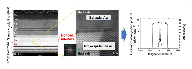
Figure 5. Cross-sectional transmission electron micrographs of the bonded interface between the single-crystal GMR film device and the polycrystalline electrode wafer (two photos at left) and magnetoresistance measured in the device post-bonding (right)
Related files
- Research Center for Magnetic and Spintronic Materials
Contacts
(Regarding this research)
-
Yuya Sakuraba
Group Leader,
Magnetic Materials Group,
Research Center for Magnetic and Spintronic Materials
National Institute for Materials Science (NIMS)
Tel: +81-29-859-2708
E-Mail: SAKURABA.Yuya=nims.go.jp
(Please change "=" to "@") -
Kay Yakushiji
Leader of the Metal Spintronics Team
Spintronics Research Center
National Institute of Advanced Industrial Science and Technology (AIST)
Tel: +81-29-861-3251
E-Mail: k-yakushiji=aist.go.jp
(Please change "=" to "@") -
Hideki Takagi
Principal Research Manager, Device Technology Research Institute
National Institute of Advanced Industrial Science and Technology (AIST)
Tel: +81-29-861-7217
E-Mail: takagi.hideki=aist.go.jp
(Please change "=" to "@") -
Katsuya Kikuchi
Leader of the 3D Integration System Group
Device Technology Research Institute
National Institute of Advanced Industrial Science and Technology (AIST)
Tel: +81-29-861-3454
E-Mail: k-kikuchi=aist.go.jp
(Please change "=" to "@")
(General information)
-
Public Relations Office
National Institute for Materials Science
Tel: +81-29-859-2026
Fax: +81-29-859-2017
E-Mail: pressrelease=ml.nims.go.jp
(Please change "=" to "@") -
Media Relations Office
Planning Headquarters
National Institute of Advanced Industrial Science and Technology (AIST)
Tel: +81-29-862-6216
Fax: +81-29-862-6212
E-Mail: press-ml=aist.go.jp
(Please change "=" to "@")