Use of Machine Learning to Design Optimal Nanostructures to Control Heat Current in Materials
2017.04.18
National Institute for Materials Science (NIMS)
University of Tokyo
Japan Science and Technology Agency (JST)
A research team consisting of NIMS and University of Tokyo researchers developed a calculation method for identifying optimal nanostructures to either maximize or minimize the thermal resistance of target materials. This method reduced the amount of calculation by more than 90% compared to conventional methods. The team also succeeded in designing novel, non-intuitive nanostructures.
(“Designing Nanostructures for Phonon Transport via Bayesian Optimization”, Shenghong Ju, Takuma Shiga, Lei Feng, Zhufeng Hou, Koji Tsuda, and Junichiro Shiomi, Phys. Rev. X 7, 021024 , DOI: https://doi.org/10.1103/PhysRevX.7.021024)
Abstract
- A research team consisting of associate professor Junichiro Shiomi (also affiliated with the Center for Materials Research by Information Integration [CMI2] at NIMS), postdoctoral fellow Shenghong Ju, assistant professor Takuma Shiga, Ph.D. student Lei Feng—all from the University of Tokyo School of Engineering—University of Tokyo Graduate School of Frontier Sciences professor Koji Tsuda (also affiliated with the CMI2 at NIMS) and NIMS researcher Zhufeng Hou developed a calculation method for identifying optimal nanostructures to either maximize or minimize the thermal resistance of target materials. This method reduced the amount of calculation by more than 90% compared to conventional methods. The team also succeeded in designing novel, non-intuitive nanostructures.
- In thermal management applications, technologies to control thermal transport in materials by forming nanoscale structures in them has been drawing attention in recent years. Taking advantage of the ballistic behavior of phonons at the nanoscale, thermal transport is becoming more controllable (e.g., thermal resistance can be increased dramatically by creating interfaces at nanoscale intervals as in superlattice structures and nanocrystalline materials). While advancements in computational science have greatly contributed to these improvements, no study of optimal structural design had been conducted.
- The research team recently developed a new method of optimizing nanostructures by combining a method of calculating thermal transport in nanostructures and a Bayesian optimization method. This newly developed method applies to two-dimensional crystalline materials and identifies optimal structures out of numerous candidate structures by assigning a descriptor to each atom composing a nanostructure. Application of this method to materials consisting of silicon and germanium demonstrated that it can identify optimal structures by calculating only a small percentage of the total candidate structures. Contrary to expectations, it was found that among the selected structures, optimal structures that maximize thermal resistance have an aperiodic layered structure rather than a periodic superlattice structure. Moreover, it was found that the mechanism of the optimal structures can be explained by the particle and wave properties of phonons.
- This study demonstrated that materials informatics—a fusion between materials science and machine learning—is useful in the development of thermally functional nanomaterials. Given that the technology to create various new nanostructures is advancing, techniques to identify structures that maximize/minimize the thermal resistance of target materials, along with materials design, may contribute to improving the heat dissipation of optical and electronic devices, heat shielding protection for devices and the efficiency of thermoelectric conversion elements.
- This study was supported by the "Materials Research by Information Integration" Initiative, launched by the JST’s Support Program for Starting up Innovation Hub. In addition, the study was carried out in conjunction with the project entitled "Development of multifunctional and multipurpose thermoelectric devices by mechano-thermal functionalization," funded by the JST CREST program, and the project entitled "Advanced thermal transport control by phonon spectrum engineering," funded by the JSPS Grants-in-Aid for Scientific Research (B).
- This study will be soon published online in Physical Review X.
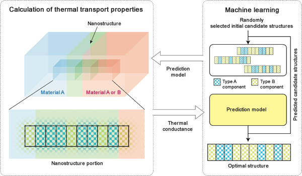
Figure: Schematics showing a calculation method for identifying nanostructures that either maximize or minimize thermal resistance.
Related files
- Research and Services Division of Materials Data and Integrated System (MaDIS)
Conacts
(Regarding this research)
-
Junichiro Shiomi
Associate professor, Department of Mechanical Engineering, School of Engineering, University of Tokyo
Tel: +81-3-5841-6283
E-Mail: shiomi=photon.t.u-tokyo.ac.jp
(Please change "=" to "@")
(Regarding JST projects)
-
Innovation Hub Group
Department of Innovation Platform, Japan Science and Technology Agency
K's Gobancho, 7 Gobancho, Chiyoda-ku, Tokyo 102-8666, Japan
Tel: +81-3-6267-4752
Fax: +81-3-5214-8496
E-Mail: ihub=jst.go.jp
(Please change "=" to "@")
(For general inquiries)
-
Public Relations Office
National Institute for Materials Science
1-2-1 Sengen, Tsukuba, Ibaraki 305-0047, Japan
Tel: +81-29-859-2026
Fax: +81-29-859-2017
E-Mail: pressrelease=ml.nims.go.jp
(Please change "=" to "@") -
Public Relations Division
Japan Science and Technology Agency
5-3 Yonbancho, Chiyoda-ku, Tokyo 102-8666, Japan
Tel: +81-3-5214-8404
Fax: +81-3-5214-8432
E-Mail: jstkoho=jst.go.jp
(Please change "=" to "@") -
Public Relations Office
School of Engineering, University of Tokyo
7-3-1 Hongo, Bunkyo-ku, Tokyo 113-8656, Japan
Tel: +81-3-5841-1790
Fax: +81-3-5841-0529
E-Mail: kouhou=pr.t.u-tokyo.ac.jp
(Please change "=" to "@")