Various Organic Transistor Functions Created through Optical Drawing
—Technology May Be Applicable to Fabrication of Logical Operation Devices That Can Be Controlled by Light and Voltage—
2016.11.15
(2017.02.21 Update)
National Institute for Materials Science (NIMS)
Kyoto University
For the first time in the world, a NIMS–Kyoto University joint research group succeeded in drawing transistor circuits and other devices on thin films of photoisomers, by irradiating light onto the films.
Abstract
- For the first time in the world, a joint research group consisting of Tohru Tsuruoka, principal researcher, Ryoma Hayakawa, senior researcher, and Yutaka Wakayama, leader of the Quantum Device Engineering Group, MANA, NIMS, as well as professor Kenji Matsuda and assistant professor Kenji Higashiguchi, Graduate School of Engineering, Kyoto University, succeeded in drawing transistor circuits and other devices on thin films of photoisomers, by irradiating light onto the films. These molecules can switch back and forth between one type of isomers that act like insulators and another type of isomers that act like semiconductors when they are exposed to light. These molecular properties enabled circuit rewriting and electric current control. These findings may also be applicable to fabrication of logical operation devices.
- Photoisomerization is a change in molecular structure and electronic state as molecules are exposed to visible or ultraviolet light. The altered state of molecules after undergoing photoisomerization can be reversed into the original state by irradiating them with light of certain wavelengths. In light of this property, it was suggested a long time ago that these molecules can be applied to memory and sensor devices. In recent years, vigorous efforts were made in the development of transistor elements that respond to light, by adding photoisomers to organic transistors. However, because only trace amounts of photoisomers were added in these studies, the increase in electric current value due to photoinduction was limited to about a factor of two. In other studies, a technology to fabricate organic transistors is being developed with the approach of printing devices on flexible substrates. This method had issues in terms of miniaturization of devices and circuit design as organic molecules break easily using conventional techniques.
- This research group previously succeeded in controlling more than 1,000 times greater electric current values than conventional values by directly using photoisomers as a transistor channel layer. This success was attributed to the discovery of a new material that possesses both photoisomeric and semiconducting properties and the discovery of the fact that the material can act as a semiconductor and insulator alternately by applying light to it. In this joint research, the group further advanced these findings by drawing transistor circuits on a thin film of photoisomers that are in an insulating state. Specifically, the group irradiated a very narrow light beam onto a certain part of the thin film, and thereby converted that part into a semiconductor.
- The joint research group developed a novel setup, which made it possible to scan the UV and visible spotlights precisely at same locations. This technique enabled us to design electric circuits those are a multiple one-dimensional channels connected in parallel, optical valves to turn on/off electric current, and Y-shaped transistor channels. These elemental techniques were achieved by utilizing the unique property of the photochromic molecule, that is, the phase transition between semiconductor and insulator can be induced by alternate UV-Vis light irradiation. Based on this technique, the group succeeded in fabrication of adder circuits capable to control electric current by adjusting the strength of light irradiation and location of optical valves.
- The findings in this study not only will serve as a new method to fabricate organic transistors but also may be applied to miniaturization of devices and large scale integration that had been major challenges in the field of organic electronics. The technology also may be applicable to optical drawing of logical circuits.
- This work was supported by JSPS KAKENHI Grant Number JP15H01098 in Scientific Research on Innovative Areas “Photosynergetics”. The study was published in the online version of Nano Letters, a journal issued by the American Chemical Society, on November 15, 2016.

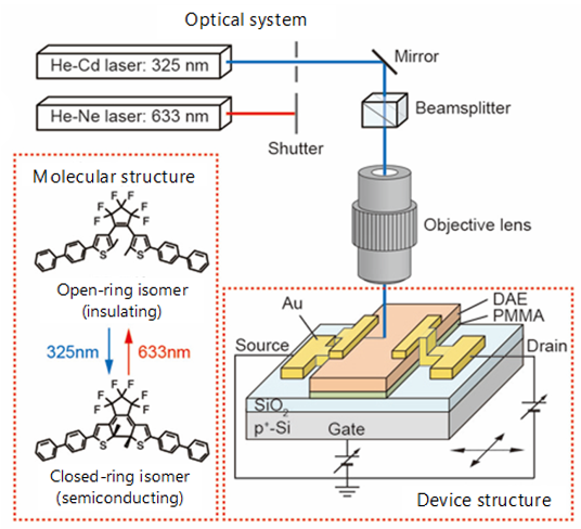
Figure. Schematics of molecular structure, device structure and light irradiation system. The molecule has a diarylethene backbone with a biphenyl group attached to both sides of the backbone. When the molecule is in the open-ring form, it behaves like an insulator, and when it is in the closed-ring form, it acts like a semiconductor. We first fabricated a thin film of open-ring isomers (insulator) on a SiO2/S substrate and attached source/drain electrodes on both sides of the thin film. The Si substrate serves as a gate electrode and the SiO2 layer functions as a gate insulator layer. If a part of the thin layer is scanned with ultraviolet light (wavelength of 325 nm), open-ring isomers there transform into closed-ring isomers (semiconductor), thereby converting that part into a transistor channel through which electric current runs. The channel can be erased by irradiating it with visible light (wavelength of 633 nm).
Related files
- MANA
Contacts
(Regarding this research)
-
Tohru Tsuruoka
Principal researcher, Nanoionic Devices Group, MANA
Tel: +81-29-860-4117
Fax: +81-29-860-4790
E-Mail: TSURUOKA.Tohru=nims.go.jp
(Please change "=" to "@") -
Yutaka Wakayama
Group Leader, Quantum Device Engineering Group, MANA
Tel: +81-29-860-4403
Fax: +81-29-860-4916
E-Mail: WAKAYAMA.Yutaka=nims.go.jp
(Please change "=" to "@") -
Kenji Matsuda
Professor, Kyoto University
Tel: +81-75-383-2738
Fax: +81-75-393-2739
E-Mail: kmatsuda=sbchem.kyoto-u.ac.jp
(Please change "=" to "@")
(Regarding public relations)
-
Public Relations Office
National Institute for Materials Science
1-2-1 Sengen, Tsukuba, Ibaraki, 305-0047, JAPAN
Tel: +81-29-859-2026
Fax: +81-29-859-2017
E-Mail: pressrelease=ml.nims.go.jp
(Please change "=" to "@")
Same Keywords
-
Development of an Organic Transistor Enabling Higher Density Circuit Integration
(transistor,organic)
2022.03.10
-
Controlling Friction Levels through On/Off Application of Laser Light
(organic,laser)
2017.02.13
-
3D Printing Nickel Single Crystals Using Laser Additive Manufacturing Technology
(laser)
2022.06.22
