Development of a New Technique for Growing High-Quality GaN Crystals
2020.11.12
National Institute for Materials Science (NIMS)
Tokyo Institute of Technology (Tokyo Tech)
NIMS and the Tokyo Tech developed a technique for growing high-quality GaN crystals with considerably fewer defects than those grown using existing techniques.
Abstract
- Gallium nitride crystals are a promising material for the development of next-generation power semiconductor devices. NIMS and the Tokyo Tech developed a technique for growing high-quality GaN crystals with considerably fewer defects than those grown using existing techniques. Unlike conventional techniques in which a crystal is grown directly in a solution, this technique uses a substrate coated with thin-alloy-film that prevents undesirable inclusions of the solution from being trapped within the growing crystal.
- GaN semiconductors are able to withstand stronger electrical currents and higher voltages than silicon semiconductors. These advantages have led to intensive R&D on GaN for use in next-generation power semiconductor devices for use in vehicles and other purposes. However, conventional GaN single crystal growth techniques, in which a gaseous raw material is sprayed onto a substrate, have a fundamental drawback: they cause the formation of many atomic-scale defects (including dislocations) in the crystal. When GaN crystals with dislocations are integrated into power devices, the leak current passes through the devices and causes damages them. To address this issue, intensive efforts have been made to develop two alternative crystal synthesis techniques: the ammonothermal method and the sodium flux method. In both methods, a crystal is grown in a solution containing raw materials for crystal growth. While the Na flux method have proven to be effective in minimizing the formation of dislocations, a new problem has been identified: a growing crystal incorporates inclusions (clumps of the constituents of the solution).
- In this project, we grew a GaN crystal while successively coating the GaN-seed substrate with a liquid alloy composed of raw materials for crystal growth (i.e., gallium and sodium), thereby preventing inclusions from being trapped within the growing crystal. In addition, this technique was found to be effective in significantly reducing the formation of dislocations, resulting in the synthesis of high-quality crystals. This technique allows the fabrication of a high-quality GaN substrate through a very simple process within approximately one hour.
- The technique we developed may offer a new method of producing high-quality GaN substrates for use in next-generation power semiconductor devices. We are currently verifying its effectiveness by growing small crystals. In future studies, we plan to develop it into a practical technique that will enable the synthesis of larger crystals.
- This project was led by Fumio Kawamura (Principal Researcher, High Pressure Group, Research Center for Functional Materials (RCFM), NIMS), Yelim Song (Junior Researcher, Optical Single Crystals Group, RCFM, NIMS) and Naoki Ohashi (Director of the RCFM, NIMS; also a professor at the Materials Research Center for Element Strategy, Tokyo Institute of Technology). This research was published in the July 16, 2020, issue of Crystal Research and Technology.
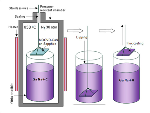
Figure 1. Schematic of the GaN crystal growth technique using the Flux-Film-Coated Liquid Phase Epitaxy (FFC-LPE) technique
Related files
- Research Center for Functional Materials
Contact information
(Regarding this research)
-
Fumio Kawamura
Principal Researcher,
High Pressure Group,
Electric and Electronic Materials Field,
Research Center for Functional Materials,
National Institute for Materials Science
Tel: +81-29-860-4428
E-Mail: KAWAMURA.Fumio=nims.go.jp
(Please change "=" to "@")
(General information)
-
Public Relations Office
National Institute for Materials Science
Tel: +81-29-859-2026
Fax: +81-29-859-2017
E-Mail: pressrelease=ml.nims.go.jp
(Please change "=" to "@") -
Public Relations Group, Tokyo Institute of Technology
TEL: +81-3-5734-2975
E-Mail: media=jim.titech.ac.jp
(Please change "=" to "@")
Same Keywords
-
Low-Resistance Buffer Layer That Paves the Way for Vertical GaN Devices on Silicon
(GaN)
2026.06.15
-
Evolving Hydrogen-storage Technology: Guidelines Developed for the Design of Anti-evaporation Catalysts
(Tokyo Institute of Technology)
2023.12.15
-
Lattice Softness: Key to the Identification of Metals with High Hydrogenation Abilities
(Tokyo Institute of Technology)
2021.08.30