Technique Enabling Rapid, Detailed Visualization of Distortions in GaN Wafers
2018.05.16
National Institute for Materials Sciences(NIMS)
A NIMS research team has developed a new wafer evaluation technique that enables simultaneous visualization of crystal-plane or lattice-plane distortions across a 2-inch, gallium nitride (GaN) semiconductor wafer at a spatial resolution of several tens of micrometers. This technique may allow wafer manufacturers to quickly and accurately evaluate the crystalline quality of GaN wafers—a candidate material for next-generation power semiconductor devices—by analyzing localized crystalline defect distributions.
Abstract
- A National Institute for Materials Science (NIMS) research team has developed a new wafer evaluation technique that enables simultaneous visualization of crystal-plane or lattice-plane distortions across a 2-inch, gallium nitride (GaN) semiconductor wafer at a spatial resolution of several tens of micrometers. This technique may allow wafer manufacturers to quickly and accurately evaluate the crystalline quality of GaN wafers—a candidate material for next-generation power semiconductor devices—by analyzing localized crystalline defect distributions.
- Energy efficient and resistant to high voltages, GaN is a promising material for use in electric vehicle motor controllers and in high-frequency devices for fifth generation mobile communications systems. The performance of these devices is greatly influenced by the number of defects in the GaN crystals. The conventional crystal-plane evaluation method employs X-ray diffraction using narrow X-ray beams. This makes the accurate measurement of these defects across an entire wafer surface very time-consuming, while the conventional and alternative approach—applying a broader X-ray beam only once to an entire wafer surface—has not allowed the collection of detailed information, such as crystal-plane orientation.
- This research team modified the conventional method of irradiating the surface of a wafer with an X-ray beam from a single direction and measuring the intensity of the diffracted X-rays. The team applied X-ray beams from two or more directions by rotating the wafer around the normal, measured the intensity of the diffracted X-rays for each direction and mathematically analyzed the data. These modifications enabled the team to simultaneously and quantitatively visualize the direction and magnitude of crystal-plane distortions across the wafer surface. It took the team only approximately 30 minutes to evaluate a 2-inch wafer for crystal-plane geometry using synchrotron X-rays at SPring-8.
- In addition to evaluation of GaN wafers, this technique is expected to be applicable to various other types of semiconductor wafers.
- This study was carried out by a NIMS research team led by Osami Sakata (Manager of the Synchrotron X-ray Characterization Group, Center for GaN Characterization and Analysis, Research Network and Facility Services Division, NIMS) in conjunction with the MEXT “Program for Research and Development of Next-Generation Semiconductor to Realize Energy-Saving Society”. A patent application has been submitted for the technique developed through this research (Patent Application No. 2018-83268).
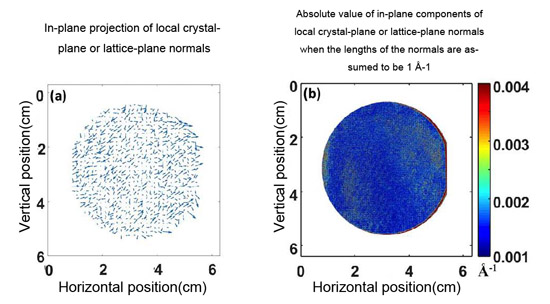
Figure to be used in the press release. (a) In-plane projected vector plot of local crystal-plane or lattice-plane normals. Direction of crystal plane distortion across a 2-inch GaN wafer. (b) The magnitude of distortion is indicated by color scale.
Related files
- Synchrotron X-ray Station at SPring-8
Contacts
(Regarding this research)
-
Osami Sakata,
Station Director,
Synchrotron X-ray Station at SPring-8,
Research Network and Facility Services Division,
National Institute for Materials Science
TEL: +81-791-58-1970
E-Mail: SAKATA.Osami=nims.go.jp
(Please change "=" to "@")
(For general inquiries)
-
Public Relations Office
National Institute for Materials Science
1-2-1 Sengen, Tsukuba, Ibaraki 305-0047, Japan
Tel: +81-29-859-2026
Fax: +81-29-859-2017
E-Mail: pressrelease=ml.nims.go.jp
(Please change "=" to "@")
Recent Press Release
-
No Need for Rare Earths or Liquid Helium! Cryogenic Cooling Material Composed Solely of Abundant Elements
2025.12.24
-
Novel Materials Design Approach Achieves a Giant Cooling Effect and Excellent Durability in Magnetic Refrigeration Materials
2025.12.19
-
Multiple Autonomous AI Systems Spontaneously Collaborate to Advance Materials Research
2025.12.10