Discovery of Crystalline Layers with Atomic Level Flatness in GaN Transistors
—A Metastable Gallium Oxide Layer at the Semiconductor–Insulator Interface Provides Insights into the Development of Next-Generation Power Devices—
2017.10.23
National Institute for Materials Science(NIMS)
A NIMS-led research team discovered a novel, metastable, gallium oxide (Ga2O3) crystal layer at the interface between a gallium nitride (GaN) crystal and an insulating layer in a GaN transistor, a promising next-generation power device. The team also observed the formation of similar Ga2O3 layers on GaN crystal surfaces, presumably due to spontaneous oxidation before the formation of an insulating layer.
(“Low-energy ion scattering spectroscopy and reflection high-energy electron diffraction of native oxides on GaN(0001),” Yoshihiro Irokawa, Taku Suzuki, Kazuya Yuge, Akihiko Ohi, Toshihide Nabatame, Koji Kimoto, Tsuyoshi Ohnishi, Kazutaka Mitsuishi and Yasuo Koide; Jpn. J. Appl. Phys. 56 128004, DOI:10.7567/JJAP.56.128004)
Abstract
- A NIMS-led research team discovered a novel, metastable, gallium oxide (Ga2O3) crystal layer at the interface between a gallium nitride (GaN) crystal and an insulating layer in a GaN transistor, a promising next-generation power device. The team also observed the formation of similar Ga2O3 layers on GaN crystal surfaces, presumably due to spontaneous oxidation before the formation of an insulating layer. This discovery may provide insight into ways of eliminating defects at the interface between a GaN crystal and an insulating layer, thereby facilitating the development of high-performance GaN transistors.
- The GaN-based metal–oxide–semiconductor field-effect transistor (MOSFET) is a promising next-generation power device. However, lower electron and hole mobility in GaN-based MOSFETs than in silicon transistors have been problems which need to be solved before MOSFETs can be put into practical use. Because the interfacial structure between the GaN crystal and the gate insulating layer has a major influence on electron and hole mobility at the interface, efforts had been made to control these interfaces by studying GaN surface cleaning processes and gate insulating layer materials. However, the processes and materials studied did not significantly improve electron and hole mobility at the interface based on electrical measurements, and the reasons for the lack of improvement remained unknown.
- The research team fabricated a transistor equipped with a silicon dioxide (SiO2) insulating layer and directly observed the interface between a GaN crystal and an SiO2 layer under an electron microscope. The team discovered the existence of a very thin (approximately 1.5 nm in thickness) Ga2O3 crystal layer which grew epitaxially on the GaN crystal. The team also found that the Ga2O3 layer is composed of a mixture of the metastable ε and γ structures, rather than the stable and widely known β structure. Because the metastable Ga2O3 crystal is flat at the atomic level, it is presumably capable of reducing interface state density, limiting the mobility of electrons and holes at the interface. In addition, the team observed a similar, epitaxially grown, metastable Ga2O3 layer of approximately 1 nm in thickness on the surface of the GaN substrate before formation of the insulating layer. Detailed analysis will be necessary to determine whether the Ga2O3 layer observed on the substrate is structurally identical to the Ga2O3 layer observed at the interface between GaN crystals and the insulating layer. These results indicate that metastable GaN crystal layers can be formed under a wide range of conditions.
- Power devices are used to switch large electric currents in automobile and train electric motors as well as in other systems. It is believed that the electric current capacity of these devices can be improved by reducing power loss. This study suggested that controlling semiconductor–insulator interfaces in GaN-based power devices may reduce electrical resistance, thereby increasing power efficiency when the devices are “on.” In future studies, we will attempt to identify conditions in which metastable Ga2O3 layers are formed, determine the relationship between such layers and the electrical characteristics of devices and achieve practical application of silicon- and silicon carbide-based next-generation power devices, in addition to MOSFETs, by optimizing their interfacial layers.
- This research project was commissioned by the MEXT "Program for the research and development of next-generation semiconductors for an energy-conserving society." Studies on the Ga2O3 layer at the MOS interface were carried out by a joint research team consisting of NIMS (the Research Center for Functional Materials (RCFM) and the Research Network and Facility Services Division (RNFS)), Fuji Electric Co., Ltd. and the University of Yamanashi, led by NIMS Research Leader Kazutaka Mitsuishi (Research Center for Advanced Measurement and Characterization (RCAMC)). This part of the study was published in the Rapid Communications section of the Japanese Journal of Applied Physics online on October 23, 2017. Studies on the native oxide films formed on a free-standing GaN substrate were conducted by a NIMS research team consisting of RCAMC, RNFS and the Center for Green Research on Energy and Environmental Materials, led by Principal Researcher Yoshihiro Irokawa (RCFM). This part of the study was published in the Japanese Journal of Applied Physics online in November 2017.
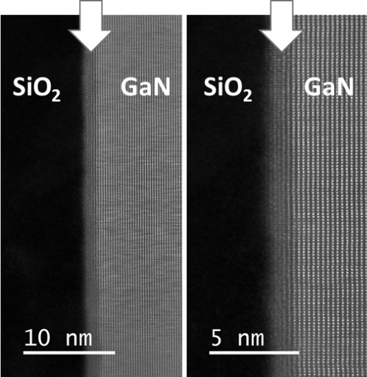
Figure: High-resolution electron microscope images of the interface between a GaN substrate and SiO2 deposited on the substrate using a PCVD method. A very thin Ga2O3 layer of a different cyclic arrangement (arrow) can be seen between the GaN substrate (lighter gray area on the right) and SiO2 (black area on the left).
Related files
- Research Center for Advanced Measurement and Characterization
- Research Center for Functional Materials
- Center for Green Research on Energy and Environmental Materials
Contacts
(Regarding measurement techniques used in this research)
-
Kazutaka Mitsuishi
Manager of the Forefront Microscopy Group, Center for GaN Characterization and Analysis,
National Institute for Materials Science
Tel: +81-29-863-5474
E-Mail: Mitsuishi.Kazutaka=nims.go.jp
(Please change "=" to "@")
(Regarding devices developed in this research)
-
Yoshihiro Irokawa
Principal Researcher, Wide Bandgap Materials Group, Research Center for Functional Materials
National Institute for Materials Science
Tel: +81-29-860-4549
E-Mail: IROKAWA.Yoshihiro=nims.go.jp
(Please change "=" to "@")
(For general inquiries)
-
Public Relations Office
National Institute for Materials Science
Tel: +81-29-859-2026
Fax: +81-29-859-2017
E-Mail: pressrelease=ml.nims.go.jp
(Please change "=" to "@")