Semiconductor Nano-integration Group
Semiconductor Materials Field
For semiconductor devices in the next generation, our goal is to develop new integration technology for semiconductor nanomaterials by “the best of both worlds”, top-down and bottom-up approaches
Group Leader:Shinjiro Hara
New integration technology for semiconductor nanomaterials and devices
Current Topics
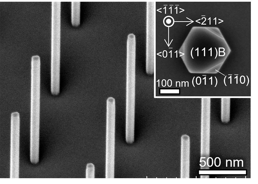
One of our group’s aims is to develop a promising device architecture of gate-all-around (GAA) transistors, in which two-dimensional transition metal dichalcogenide (TMDC) nanosheets or vertically free-standing group III-V or IV semiconductor nanowires (NW) with a large aspect ratio are utilized as suitable channel materials. Among them, vertical semiconductor NWs have attracted great attention as a building block to improve the device performance associated with the miniaturization of transistors. There are several methods reported so far to obtain vertical semiconductor NWs in the stie-controlled manner on a substrate by a bottom-up approach. In our group, we have developed the selective-area (i.e., site-controlled) growth methods for group III-V and IV semiconductor NWs on semiconductor {111} substrates. The conventional and simple method for growing group IV and III-V semiconductor NWs is the “vapor-liquid-solid (VLS)” method with a metal catalyst, in which “supersaturation” of source materials at the interface between a solid substrate and eutectic liquid nano-droplets is used as a driving force for crystal growth. We have recently demonstrated the “site-controlled VLS growth” of Ge NWs heterogeneously on Si (111) substrates, in which periodic circular disk patterns of Au thin film catalysts fabricated by electron beam (EB) lithography and lift-off are utilized. [1,2] In the case of III-V semiconductor NWs, however, we can also use “faceting phenomenon” on the top and sidewall surfaces of NWs [ 3 ] as their growth rates are markedly different between crystal facet surfaces, which depend on a partial pressure of group V source gas and growth temperature. This “faceting growth” enables us to realize the “site-controlled growth” of III-V semiconductor NWs (Fig. 1) without any use of metal catalysts, using the periodic array of circular openings formed by EB lithography and etching in the growth-inhibiting dielectric SiO2 films deposited on Si, GaAs, and InP substrates. [3-6]
References
-
Collected Abstracts of ISCSI-X, TuB3-4,63–64 (2025). DOI: https://tsys.jp/iscsi/2025/program/program.html
Group members
-
Shinjiro Hara
- Group Leader