Nanostructured Semiconducting Materials Group
Semiconductor Materials Field
New functional semiconductor nanodevices using novel physical properties
Group Leader:Naoki Fukata
Next-Generation Semiconductor, Nanostructures and devices
Current Topics
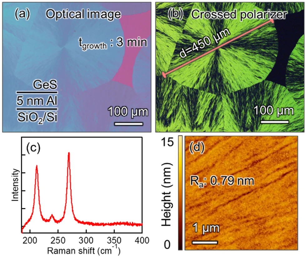
Group IV chalcogenides such as silicon sulfide (SiS), germanium sulfide (GeS) and tin sulfide (SnS) are new two-dimensional layered materials that can be used in semiconductor devices. To elucidate the growth process of GeS and enable its control, we investigated the effects of GeS buffer layers and metal catalysts, in addition to growth on insulating substrates and Si substrates. Al was used as the metal catalyst.
Without a metal catalyst, crystal growth exhibited a square shape reflecting the GeS crystal structure. However, on the Al catalyst, crystal growth spread out into a circular shape. This can be attributed to the catalytic effect of Al accelerating the growth rate, causing crystallization to proceed radially outward from the nucleation site. Currently, we are exploring growth conditions that enable the realization of single-crystal growth with fewer defects by further controlling the crystal growth rate.
We also investigated the growth of SnS thin films by molecular beam deposition (MBE) using a plasma-cracked sulfur (S) source to explore the influence of S chemical activity. Plasma activation of S enabled the successful formation of stoichiometric and crystalline SnS at moderate substrate temperatures, while uncracked S8 resulted in S-deficient films. Furthermore, under higher S flux and lower thermal budget, crystalline SnS2 formation was also observed.
References
Group members
-
Naoki Fukata
- Deputy Director of MANA
- Field Director of Semiconductor Materials Field
- Group Leader
-

Wipakorn Jevasuwan
- Senior Researcher
-
Ryo Matsumura
- Senior Researcher