Semiconductor Device Group
Semiconductor Materials Field
Process and material innovation with a focus on interface control for future semiconductor devices
Group Leader:Takuji Hosoi
Development of nanosheet formation, gate stack engineering, and interface control technologies for post silicon semiconductor devices
Current Topics
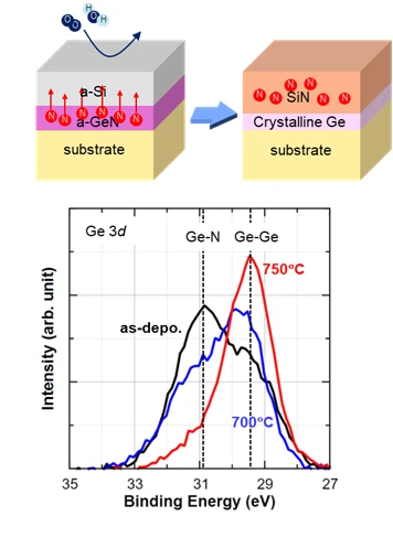
To further advance CMOS scaling, high-crystalline and atomically flat semiconductor nanosheets with high carrier mobility are indispensable. Theoretical study on electron mobility in 2‑nm‑thick nanosheets suggest that Ge(111) nanosheets may exhibit mobilities more than an order of magnitude higher than those of Si nanosheets [ 1 ]. However, the fabrication of such ultrathin Ge nanosheets remains challenging, and the predicted high mobility has yet to be experimentally demonstrated.
It has been reported that vacuum annealing of plasma‑nitrided GeN/Ge structures induces selective nitrogen desorption and recrystallization of Ge [ 2 ]. Based on this insight, we explore a novel method for forming Ge nanosheets. A stacked structure consisting of a GeN film and an Si capping layer was fabricated on a sapphire substrate, and Ge nanosheet formation was achieved by driving nitrogen atoms from the GeN layer into the Si capping layer through vacuum annealing (Fig. 1). This achievement opens a pathway toward the fabrication of ultrathin, high‑quality Ge nanosheets.
References
Group members
-
Takuji Hosoi
- Group Leader