2D Semiconductor Group
Semiconductor Materials Field
We develop high-quality 2D semiconductors and device fabrication processes for next-generation electronics.
Group Leader:Yasumitsu Miyata
Strain-Engineered 2D Semiconductors: Diameter-Tunable Janus Nanoscrolls and Uniform Thermal-Strain Control in Monolayer WSe2
Current Topics
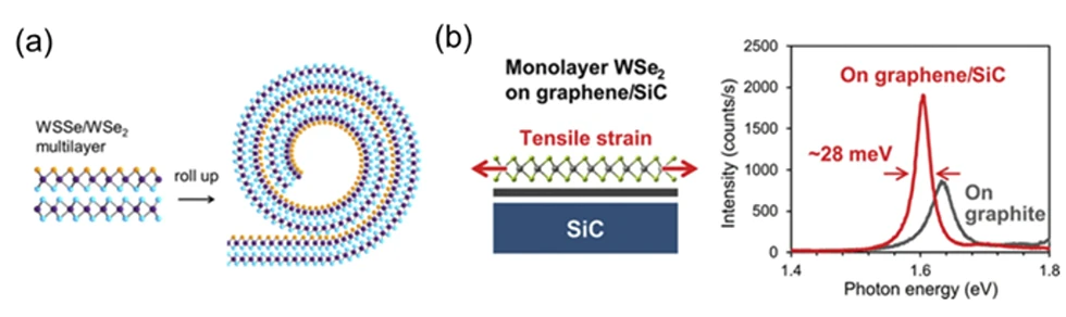
1. Diameter-tunable nanoscrolls from Janus WSSe/WSe2 heterostructures.
Transition metal dichalcogenide (TMD) nanoscrolls are promising for exploring curvature- and chirality-dependent phenomena, yet systematic diameter control and structure–optics correlation are still limited. Building on our earlier finding that a Janus TMD monolayer can self-roll due to intrinsic strain from out-of-plane asymmetry, we demonstrate diameter-tunable nanoscrolls formed from Janus WSSe/WSe2 heterostructures (Fig. 1a). Embedding a monolayer Janus WSSe within a multilayer stack promotes roll-up and enables continuous tuning of scroll diameter from ~10 nm to ~1 μm. Scanning transmission electron microscopy confirms crystallinity and compositional uniformity, indicating that the heterostructure survives large bending without phase separation. Optical measurements reveal anisotropic Raman responses and SHG modulation associated with uniaxial strain. These results establish a materials basis for studying bending responses and for designing mechanically programmable optical functionalities.
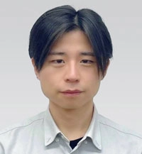
2. Uniform thermal-strain engineering of monolayer WSe2 on graphene/SiC(0001).
Thermal strain is a powerful knob for tuning TMD band structure and exciton scattering, but conventional substrates often cause inhomogeneity via roughness and charged impurities. Using van der Waals epitaxy on graphene/SiC(0001), we introduce a spatially uniform thermal strain into monolayer WSe2. Relative to WSe2 grown on graphite, the PL peak red-shifts and the linewidth narrows by ~30% (Fig. 1b), consistent with tensile-strain-induced band modulation and reduced exciton scattering. The small thermal expansion of SiC and disorder-screening by interfacial graphene likely underpin the improved uniformity and reduced inhomogeneous broadening. By offering a clean, scalable strain-control scheme, this approach can be extended to diverse vdW heterostructures for strain-engineered optoelectronics.
References
-
Tunable-diameter nanoscrolls from Janus WSSe/WSe2 heterostructures, ACS Nano,19, 34918–34927 (2025). DOI: https://pubs.acs.org/doi/10.1021/acsnano.3c05681
-
Improved strain engineering of monolayer transition metal dichalcogenides via van der Waals epitaxy on graphene/SiC(0001), Nano Lett.,25, 12851–12858 (2025). DOI: https://pubs.acs.org/doi/10.1021/acs.nanolett.5c02492
Group members
-

Yasumitsu Miyata
- Group Leader
-
Ryotaro Sakakibara
- Researcher