Photonics Nano-Engineering Group
Semiconductor Materials Field
Photonics Nano-Engineering group focuses on the study of novel functionalities originating from interfacial electronic/vibronic excitations and photonic properties in nano and micrometer-scale systems
Group Leader:Tadaaki Nagao
Surface nanotechnology and material science for sensing and photoenergy applications
Current Topics
We study rational design of the devices and synthesis of wavelength conversion and photoenergy converted devices adopting lithographic dielectric nanostructures and chemical nano-synthesis routes. For example we study high-sensitivity and precise sensing methods working in the near to the mid infrared region, including surface-enhanced infrared spectroscopy supported by all-dielectric nanophotonic materials. We also develop infrared photothermal spectroscopic devices as well as UV and NIR photodetectors and light emitters.
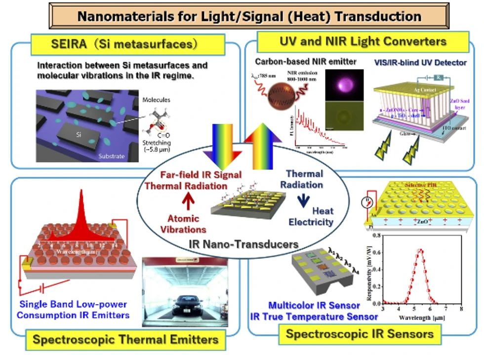
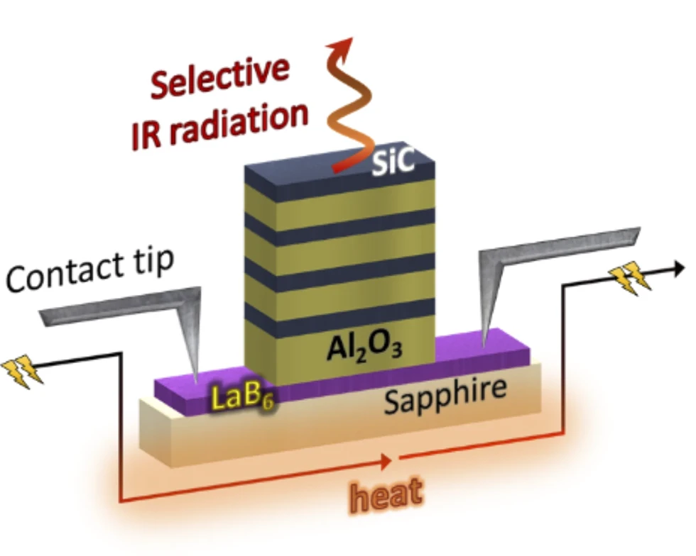
We realized a narrowband thermal emitters when it is fabricated with refractive dielectrics and highly conductive refractory boron-based ceramics that can sustain well above 1000 deg C. The combination with appropriate perfect absorber design and low-loss metals will open a new avenue for innovative technologies not only in true-temperature thermography, but also create industry seeds for low-temperature rapid heating by material-specific infrared heaters.
References
-
ACS Appl. Mater. Interfaces16(17), 22312 (2024). DOI: https://pubs.acs.org/doi/10.1021/acsami.3c18035
Group members
-

Tadaaki Nagao
- Group Leader
-

Wataru Hayami
- Principal Researcher
-

Keisuke Watanabe
- Researcher
Activities
- Mar. 3, 2025Keisuke Watanabe Researcher received the Excellence Award of the Konica Minolta Imaging Science Encouragement Award