About 2D Semiconductor Group
Science and applications of two-dimensional materials
Our research group focuses on nanomaterials with characteristic structures on the nanometer scale, which exhibit unique properties distinct from those of conventional three-dimensional materials. In particular, we study atomically thin two-dimensional materials—typically only one to a few atomic layers thick—with the aim of advancing both fundamental understanding and application-oriented research toward next-generation semiconductor devices.
Specialized Research Field
Development of high-quality two-dimensional semiconductors for electronics applications
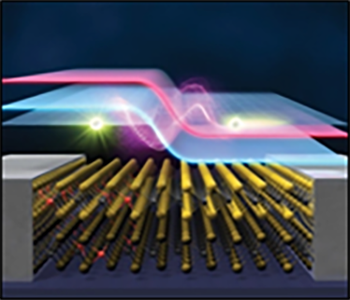
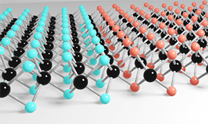
Transition metal dichalcogenides (TMDs), a representative class of two-dimensional semiconductors, have attracted significant attention as candidates for next-generation semiconductor channels due to their atomically thin structure, atomically flat surfaces, and excellent electronic transport properties even at thicknesses below 1 nm. However, for practical device applications, there remain many technical challenges, including improving crystal quality, controlling doping, forming low-resistance contacts, fabricating high-quality gate insulators, and integrating these components through scalable processes.
Our research group aims to address these challenges by advancing growth techniques and developing fabrication processes, with the ultimate goal of establishing the key technologies required for future transistor architectures.
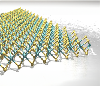
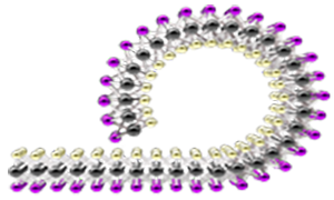
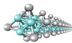
Exploration and functional development of novel nanomaterials
To fully exploit the potential of nanomaterials and impart novel functionalities, precise control over their structure is essential. For example, two-dimensional materials can be transformed into nanotubes or nanoscrolls by rolling their sheet-like structures, introducing new degrees of structural freedom. Furthermore, both two-dimensional and one-dimensional materials allow for the formation of new crystal systems with unique periodicities through heterojunction formation and intercalation of atoms or molecules into nanoscale voids.
Our group focuses on heterostructures based on transition metal dichalcogenides (TMDs) and nanowires composed of transition metal monochalcogenides, aiming to develop advanced methods for structural control and to explore the novel physical functions that emerge from these nanostructures.
Group Members