Production of large, high-quality single crystals for optical applications using the pulling method
Group in charge
Optical Single Crystals Group
SHIMAMURA, Kiyoshi
VILLORA, Garcia

The technologies used at this center can be broadly divided into synthesis/manufacturing technology and evaluation analysis technology.
This page specifically focuses on Synthesis and processing methods. Method for Characterization and measurements is at 【another page 】.
There is also a wide range of Synthesis and processing technologies. First, it is a means of obtaining the desired material by reacting or melting substances at high temperatures, using a so-called "furnace. " On the other hand, it is a means of synthesizing materials at relatively low temperatures, that is, using chemical methods that can be imaged from beakers or flasks. It provides a means of synthesizing substances from liquids such as aqueous solutions. There are also processes that use liquids and do not involve a dissolution step. An example of this is the process of dispersing powder into a liquid. Dispersion processes are of great importance in materials synthesis.
Another method is to synthesize materials by depositing vaporized raw materials as solids on a substrate. This process of precipitating a solid phase from a gas phase is often used for high-purity synthesis in a vacuum environment. Furthermore, this center will utilize shape forming technology such as microfabrication technology for device formation.
We also have equipment available for use by outside organizations. If you are interested, please inquire.
Solid and melt processes / high temperature processes
We will introduce manufacturing processes that use high temperatures, such as solid phase reactions and melt processes, at this center.
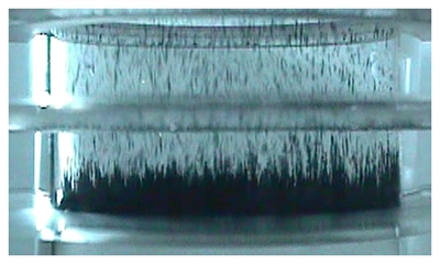
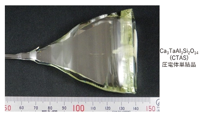
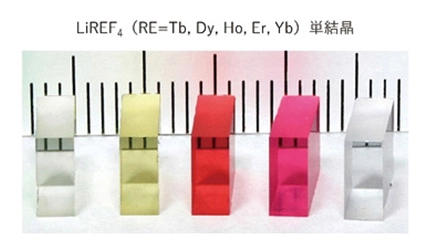
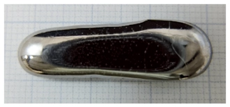
It is a process that produces large single crystals from melted liquid at high temperatures.
Group in charge
Optical Single Crystals Group
SHIMAMURA, Kiyoshi
VILLORA, Garcia
Group in charge
Optical Single Crystals Group
NAKAMURA, Masaru
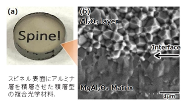
This is the process of creating ceramics by densifying powder at high temperatures.
Group in charge
Optical Ceramics Group
SUZUKI, Tohru
Group in charge
Polycrystalline Optical Material Group
MORITA, Koji
This is a synthesis method that involves reacting a solid at high temperature with a gas. A typical example is nitride synthesis using ammonia.
Group in charge
Advanced Phosphor Group
TAKEDA, Takashi
Group in charge
Electro-ceramics Group
SUEHIRO, Takayuki
Group in charge
Amorphous Material Group
SEGAWA, Hiroyo
We would like to introduce the liquid phase process at this center.
This is a process for controlling the behavior of fine particles dispersed in a liquid to bring out material properties.
Group in charge
Optical Ceramics Group
SUZUKI, Tohru
Group in charge
Nanophotonics Group
FUDOUZI, Hiroshi
Solid-phase materials are synthesized by precipitating raw materials dissolved in a solvent.
Group in charge
Electro-ceramics Group
SAITO, Noriko
Group in charge
Optical Ceramics Group
NAKANE, Takayuki
Group in charge
Amorphous Material Group
SEGAWA, Hiroyo
HAYASE, Gen
A synthesis method that induces chemical reactions and mass transport by applying an electric field to the interface between a solution and a solid.
Group in charge
Amorphous Material Group
SEGAWA, Hiroyo
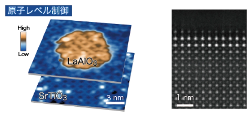
We will introduce vapor phase growth at this center.
This is a process in which raw materials are vaporized in a vacuum and then deposited and crystallized on a wafer.
Group in charge
Semiconductor Epitaxial Structures Group
MANO, Takaaki
OHTAKE, Akihiro
KAWAZU, Takuya
Group in charge
Amorphous Material Group
OGAKI, Takeshi
This is a process in which raw material molecules carried by a gas flow react on the substrate surface and precipitate and crystallize.
Group in charge
Semiconductor Defect Design Group
TERAJI, TokuyukiWATANABE, Kenji
Group in charge
Ultra-wide Bandgap Semiconductors Group
KOIZUMI, SatoshiLIAO, Meiyong
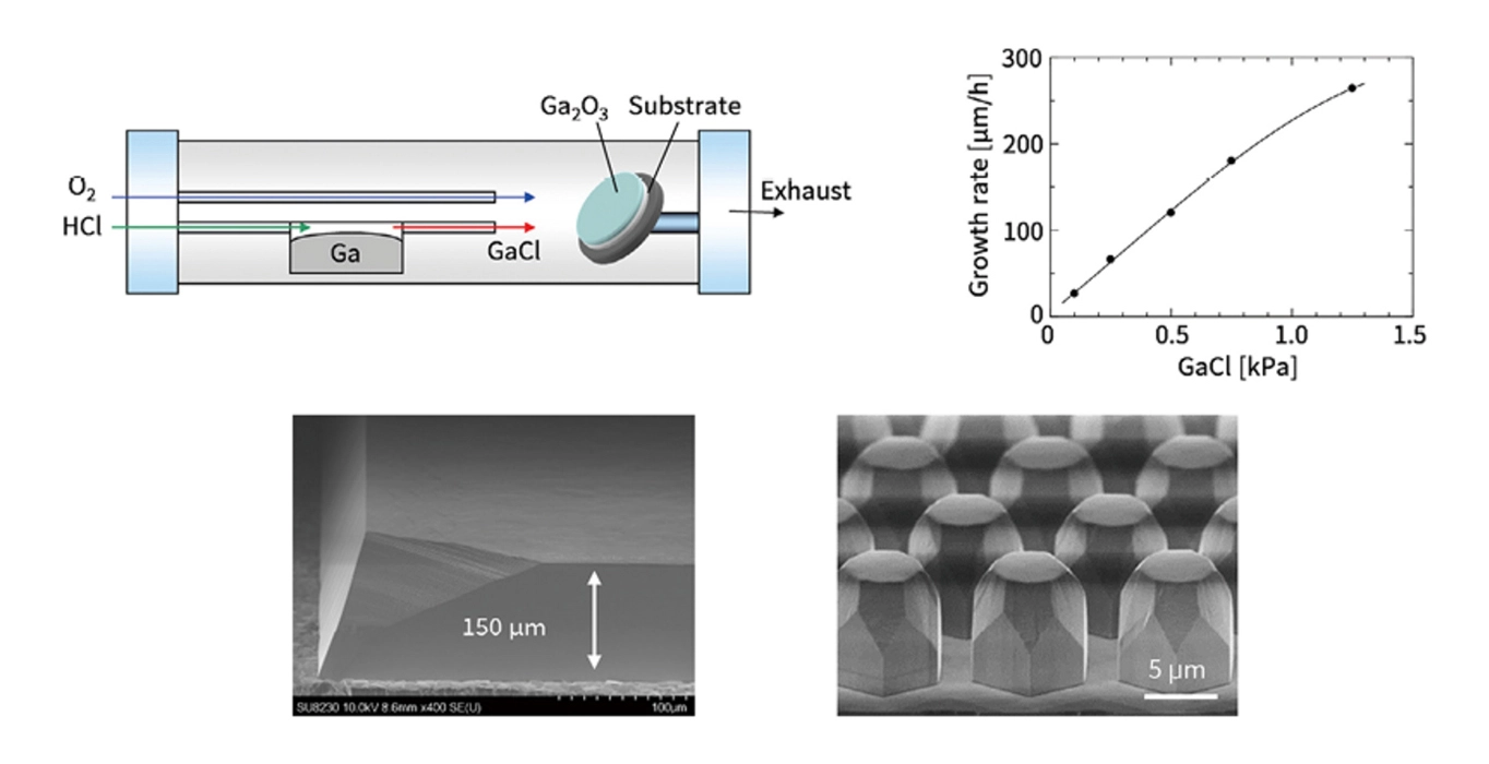
This is a crystal growth method in which raw metal is transported onto a substrate as chloride gas and crystals are deposited on the substrate.
Group in charge
Ultra-wide Bandgap Semiconductors Group
OSHIMA, Yuichi
This is a thin film growth process in which raw materials evaporated by laser pulse irradiation are deposited and crystallized on a substrate wafer.
Group in charge
Electro-ceramics Group
ADACHI, YutakaSHIMIZU, TakaoOHSAWA, Takeo
Group in charge
Nano Electronics Device Materials Group
NAGATA, Takahiro
Raw materials vaporized using plasma are deposited on a wafer to grow crystals and synthesize thin film crystals.
Group in charge
Electro-ceramics Group
SHIMIZU, TakaoOHSAWA, Takeo
Group in charge
Nano Electronics Device Materials Group
NAGATA, Takahiro
Fabrication processes used in this center
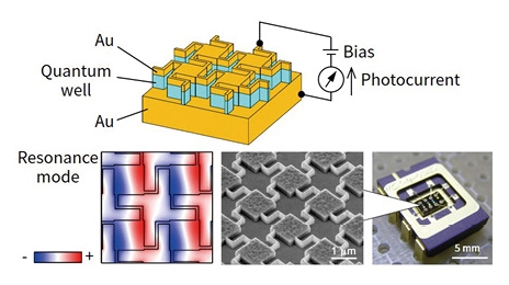
It is a process in which fine structures are formed on the surface of a wafer or thin film using pattern formation on a resist film using electron beams or light.
Group in charge
Nanophotonics Group
IWANAGA, Masanobu
Group in charge
Semiconductor Epitaxial Structures Group
MIYAZAKI, Hideki
Group in charge
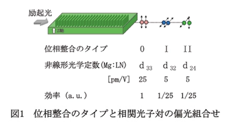
Quantum Photonics Group
KURIMURA, Sunao
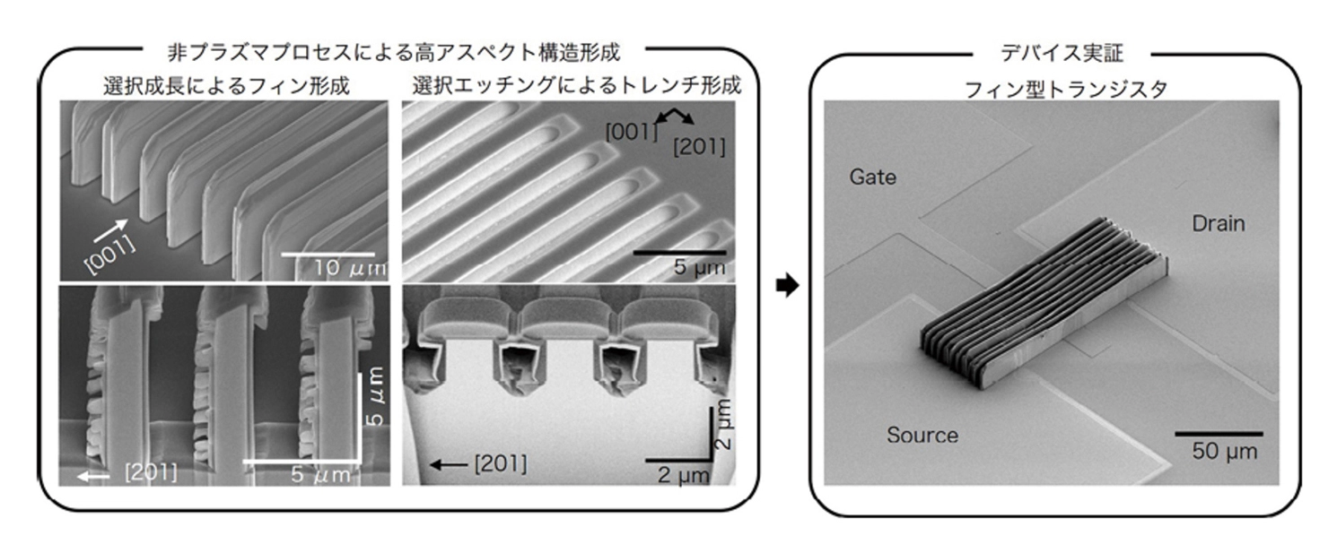
This method uses acid/alkaline solutions, plasma, etc. to remove the sample surface by dissolving or evaporating it and giving it the desired shape.
Group in charge
Ultra-wide Bandgap Semiconductors Group
OSHIMA, Takayoshi
Group in charge
Nanophotonics Group
IWANAGA, Masanobu
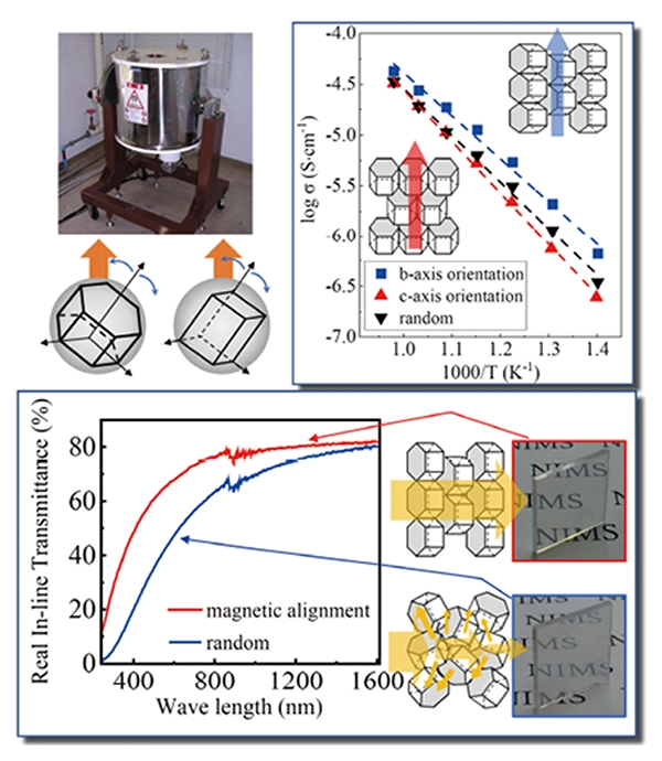
By applying a magnetic field to powder, etc., particle aggregation and orientation are controlled.
Group in charge
Optical Ceramics Group
HIROTA, NoriyukiSUZUKI, Tohru