 SEGAWA.Hiroyo@nims.go.jp
The formation of films by anodic oxidation has been known for a long time, but in this research, we have promoted the formation of high-gloss anodic oxide films that are different from existing coloring by using AC anodic oxidation. In existing technology, nanometer-sized pores are formed in a direction perpendicular to the substrate, and color is controlled by introducing pigments into the pores. The pigments have poor durability at high temperatures and are prone to fading.
On the other hand, the film obtained in this research is composed of layers of nanometer-thick alumina films, and it is possible to control the color by electrochemically controlling the thickness of each film.
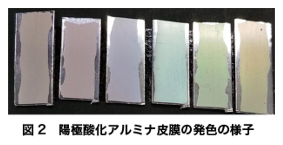
Figure 2 shows the appearance of the alumina film prepared under different conditions. It has been confirmed that it is possible to control the color by controlling the voltage. Since the color is generated by the alumina itself, it is highly durable even at high temperatures. In addition, due to the layered structure, it is difficult for cracks to develop and the film has high toughness.
Amorphous Material Group | Research Center for Electronic and Optical Materials

Amorphous Material Group
Group Leader
Group members
AIM and GOAL
Amorphous materials have a network structure in which atoms are irregularly arranged. The density of the material depends on the atomic arrangement, resulting in that various physical properties such as refractive index, dielectric constant, ionic conductivity, and elastic modulus are controlled.
By controlling the sub-nano- to nanometer-sized spaces in amorphous materials, we aim to create functional materials that contribute to technological innovation for energy and resource conservation, and to propose materials that will help realize greater efficiency and affluence by linking cyberspace and humans through the achievement of Society 5.0.
APPROACH
The group focuses on functional properties of amorphous materials by controlling the atomic arrangement and local and network structures in amorphous materials. In addition to the melting method, we also synthesize the amorphous materials by solid-phase reactions using the sparkling plasma sintering method and liquid-phase reaction processes using the sol-gel method and electrochemical methods.
The group aims to obtain functional amorphous materials by controlling the sub-nano and nano-meter sized spaces by various methods.
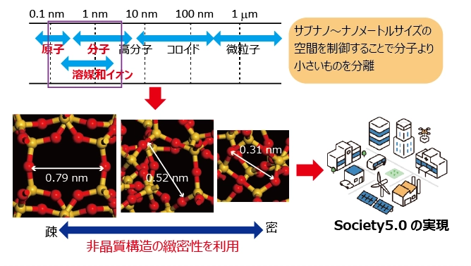
Fig 1 Our research targets.
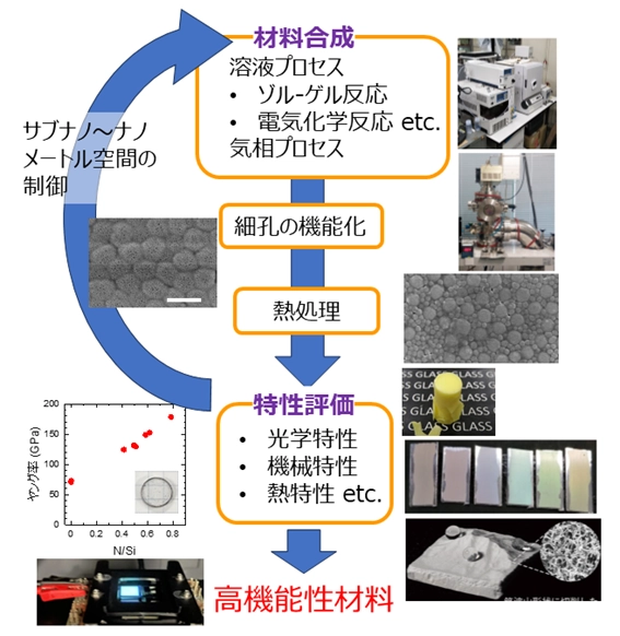
Fig 2 Overview of our research approach.
SEGAWA, Hiroyo / Group Leader
Functional exploration of glass and amorphous materials
Overview
Oxide glasses are easy to produce and are widely used as transparent, chemically resistant materials. Glasses in which the oxygen in oxide glasses is replaced by nitrogen are known as oxynitride glasses, and it is known that the introduction of nitrogen improves various physical properties such as chemical resistance, heat resistance and mechanical properties such as hardness, as well as optical properties such as refractive index.
However, when using nitride raw materials to introduce nitrogen, it is difficult to form a stable melt due to decomposition of the source nitrides during heating, and the bulk properties have not been sufficiently investigated.
In this study, we aim to produce functional oxynitride glasses by introducing nitrogen through heat treatment in an ammonia atomosphere and investigate the bulk properties of various oxynitride glasses.
We are also using anodization to create amorphous oxides, and are also working on developing functional materials with a focus on optical, mechanical and electrical properties.
Characteristics
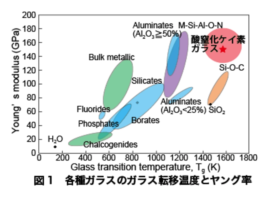
- By producing silicon nitride glass, we have achieved a glass transition temperature about 200°C higher than that of silica glass, as well as a higher refractive index and Young's modulus.
- We have succeeded in producing luminescent glass using silicon oxynitride glasses.
- We have created phosphorus nitride glass and succeeded in solidifying cesium chloride, which is difficult to solidify as radioactive waste.
- By controlling the structure of anodized alumina film, we have achieved a variety of colors without the use of dyes.
Major reserch 1
Major reserch 2
An increase in nitrogen concentration in silicon nitride glass has been found to be associated with an increase in glass transition temperature and Young's modulus. Figure 1 shows the relationship between glass transition temperature and Young's modulus of various glasses. The currently available silicon nitride glass is in the red region. It has a higher glass transition temperature and higher Young's modulus than fused silica.
It is a transparent glass that is durable at high temperatures and is expected to be used in substrates for lithography, lenses for automotive and high-intensity projectors, etc. It is possible to absorb ultraviolet rays and emit visible light using a luminescent silicon oxynitride glass film doped with Eu ions. It is expected to be used as a wavelength conversion material that can efficiently utilize ultraviolet light by coating it on the cover material of solar cells.
It has been confirmed that phosphorus oxynitride glass has higher chemical durability than phosphate glass, and it is expected to be used as a glass for solidifying radioactive waste caesium chloride and as an electrolyte material for batteries as an ion conductor.
Summary
Silicon oxynitride glass technology:
As a glass material with higher heat resistance than silica glass, it has potential applications in components that require heat resistance. In addition, fluorescent glass has the potential to become a functional film that can help improve the efficiency of solar cells as a glass film.
Phosphorous oxynitride glass technology:
As a glass with high chemical durability and ion solubility similar to phosphate glass, it is expected to be used as a glass matrix for radioactive waste solidification and as a proton-conducting glass.
Anodization technology:
It is expected to be used as a coloring agent by utilizing its colorability. In addition, it is possible to form a tough film by AC electrolysis, and it can be applied to a film that is less likely to crack than a DC electrolysis film.
OGAKI, Takeshi
Application of rock-salt nitride semiconductors to optical and electronic devices
Overview
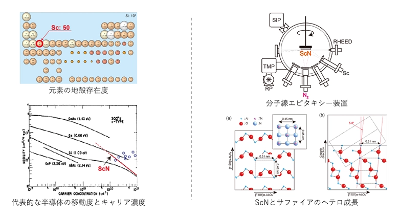
With the progress of research on optical and electronic devices of group IIIb nitrides such as GaN, ScN is expected to be applied to the field of semiconductors.
ScN is a group IIIa nitride with a rock-salt crystal structure. ScN is an n-type semiconductor with a high carrier concentration generated from defects due to a large non-stoichiometric composition, and exhibits high electron mobility.
Since (111)-oriented rock-salt ScN and c-axis oriented wurtzite GaN are lattice-matched and the lattice constants of rock-salt ScN and zinc-blende GaN are also the same, so it is expected that ScN will be integrated with GaN-based semiconductors, such as GaN/ScN heterostructures utilizing the small lattice mismatch.
Characteristics
- Exploration of new nitride semiconductor materials
- Heteroepitaxial growth of rock-salt nitrides
- Controlling the physical properties of ScN with large non-stoichiometric compositions
- olid solution and stacking of rock-salt nitrides with GaN-based semiconductors
Major reserch
Sc is classified as an expensive element due to its limited applications; however, Sc is a resource-rich material that is abundantly available on Earth. ScN has a rock-salt crystal structure and exhibits high electron mobility despite being an n-type semiconductor with high carrier concentration generated from defects due to its non-stoichiometric composition. However, there are many unknowns regarding its physical properties.
In this study, we synthesize high-quality ScN films by molecular beam epitaxy, clarify their physical properties, and investigated the possibility of applying rock-salt semiconductors to semiconductor devices.
Summary
By optimizing the growth conditions, we succeeded in heteroepitaxial growth of high-quality ScN thin films and clarified that ScN has a large non-stoichiometric composition, and that its optical and electronic properties change significantly depending on the composition.
Realization of control of non-stoichiometric composition and control of physical properties by doping will lead to the application of ScN to semiconductor devices.
HAYASE, Gen
Facile Preparation and Versatile Applications of Flexible Monolithic Porous Materials
Overview
Various types of porous materials have been widely studied and used for many years, each taking advantage of its unique physical properties.
For porous materials prepared by the sol-gel method, precise control over the chemical composition as well as the micro- and nanoscale framework and pore structures allows the development of materials tailored for specific applications, such as thermal insulation, diffuse Reflecting Materials, adsorption and separation media, battery materials, catalysts, and substrates for cell culture.
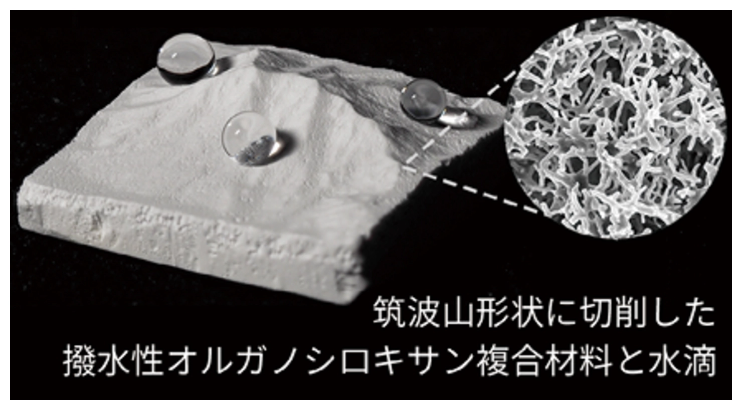
Monolithic porous materials based on organosiloxanes (such as silicones) are particularly promising for a wide range of advanced applications due to their flexibility and chemical stability. In addition, by incorporating nanomaterials into and onto the porous framework, our research aims to create novel properties not observed in conventional plastics or ceramics.
Characteristics
- Flexible macroporous materials with high reproducibility via a simple process
- Formation of unique microstructures and mechanical property control through nanoceramic compositing
- Compatible with CNC microfabrication using a milling machine
- Application to thermal management materials with excellent thermal insulation and optical properties
- Usable for three-dimensional cell culture, including spheroids and organoids
Major reserch
The sol-gel process, accompanied by phase separation, allows the formation and control of various fine structures in monolithic porous materials. However, the efficient formation of organosiloxane materials, which are typically hydrophobic, from aqueous sol systems requires carefully designed techniques. By developing processes that allow simple control of phase separation, we have successfully fabricated bulk materials with high reproducibility and minimal defects at various scales.
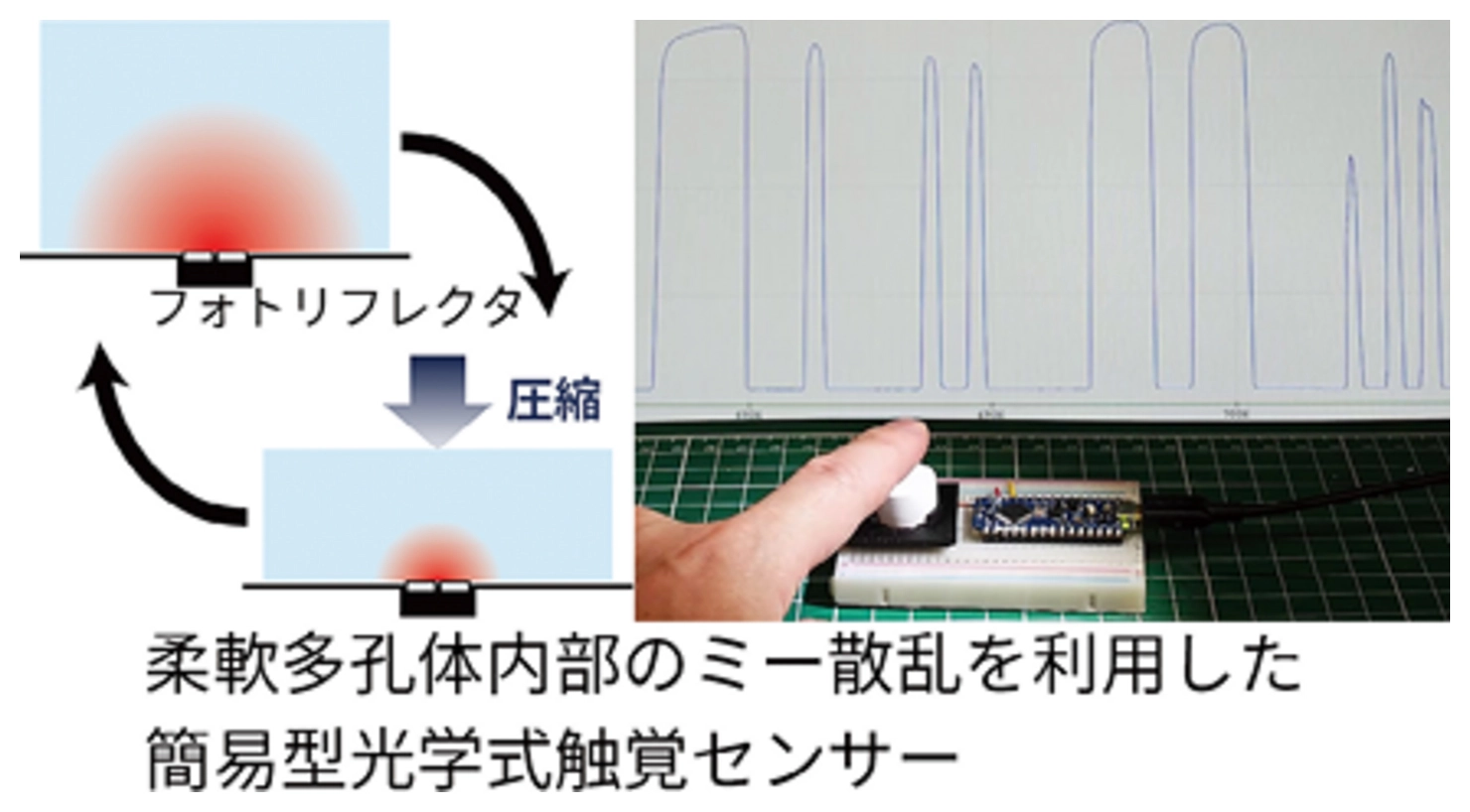
By utilizing the deformability of flexible porous materials, we have developed new applications in a wide range of fields. These include thermal insulation materials that maintain their performance regardless of shape change, substrates for giant vesicle (liposome) formation that can be used in a manner similar to squeezing a sponge, and optical materials for tactile sensors that also function as interfaces.
We are also developing bulk materials with enhanced strength by incorporating nanomaterials into the fine skeleton of monolithic porous structures. These composite materials exhibit significantly improved impact and wear resistance compared to their non-composite counterparts. As a result, precision machining, previously a challenge for low bulk density porous materials, has become feasible.
Composite materials with organosiloxane-based surface compositions exhibit excellent water repellency and biocompatibility, leading to the development of three-dimensional cell culture substrates. In addition, we are actively exploring their potential as optical materials, taking advantage of the visible light transmission and infrared radiation properties of organosiloxanes, as well as the diffuse reflection properties derived from their porous structures.
Summary
Although organosiloxanes have a higher raw material cost than conventional plastics and ceramics, they exhibit a variety of unique properties that are not found in either material. As highly functional materials, we are particularly focused on developing new applications in the bio and medical fields.
AMEKURA, Hiroshi
Collective shape elongation of metal nanoparticles dispersed in glass: realized by ultra-high energy ion irradiation
Overview
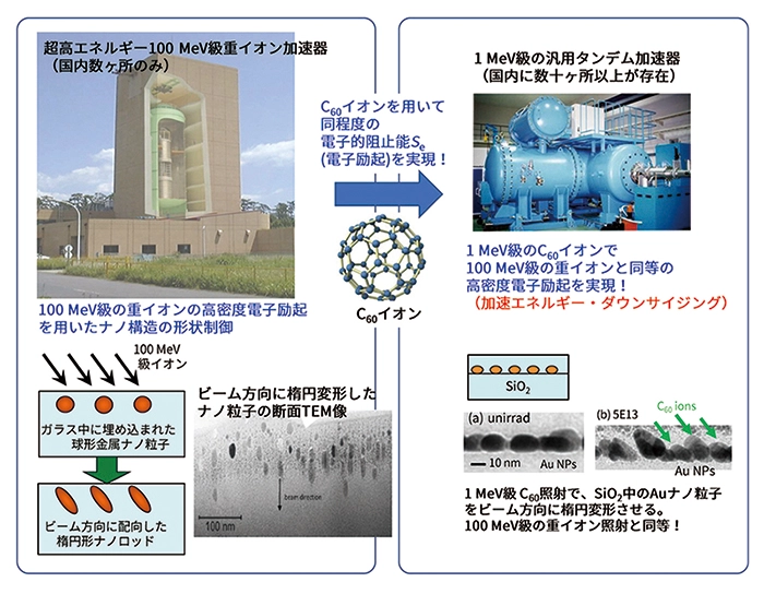
For these decades, the phenomena in which ultra-high energy heavy ion irradiation induces collective shape changes of nanostructures, such as nanoparticles and nanopillars, from spheres to spheroids and from cubes to cuboids, has been extensively investigated, and some advances have been made for understanding the phenomena. It has been confirmed that the shape changes require at least tens of MeV of energy when using monatomic ions. This too high energy is a barrier to the practical application of this technology.
In this study, we demonstrated that similar shape changes can be induced in nanostructures with acceleration energies such as MeV (i.e., energy that is two orders of magnitude lower) by using cluster ions such as C60 instead of monoatomic heavy ions. It is a proposal for a technology that should be called "downsizing of acceleration energy".
Characteristics
- Although the advantages of nanostructure shape-change technology by irradiating with ultra-high-energy heavy ion beams of ≈100 MeV were known, the accelerators that could generate this energy range were limited in Japan to a few large-scale facilities, making it difficult to develop them into industrial applications.
- In this study, by using C60 ions of the 1 MeV class, we have achieved the shape changes of nanostructures similar to those by 100 MeV class monoatomic heavy ions.
- There are dozens of 1MeV-class accelerators in Japan, and the barriers to industrial applications have been greatly lowered.
Major reserch
The upper left of the figure shows an example of a 100 MeV class heavy ion accelerator. In this example, a seven-floor building constitutes an accelerator. Such a large accelerator is required to generate a 100 MeV class beam, and there are only a few such facilities in Japan. The results of irradiating 100 MeV ions to metal nanoparticles dispersed in glass are shown in the lower left figure. The spherical nanoparticles extend in the direction of the beam and transform into nanorods. The upper right of the figure shows an example of a 1 MeV tandem accelerator. There are more than dozens of accelerators of this level in Japan, and they are also used in industrial applications. In this study, we have shown that it is possible to induce the shape elongation of nanoparticles even in a 1 MeV class accelerator using C60 ions (lower right), which greatly lowers the barrier to industrial application.
Summary
While the shape changes of nanostructure were believed to be attained only by an extremely rare 100 MeV-class ion accelerator, it has been clarified by us that the shape changes can be also realized with C60 ions in many 1 MeV-class accelerators. However, it should be noted that the irradiation of the two ion species (C60 ions and monatomic ions) does not induce perfectly equivalent effects. Rather, C60 ion irradiation has a higher sputtering rate and may destroy nanostructures depending on the conditions. To avoid this, we need further understanding of the interaction between MeV C60 ions and solids.
Current Members (as of 2026)
Graduate Research Assistant
SUEMORI, Shuto SUEMORI.Shuto@nims.go.jp
Project Technical Staff
SEKINE, Satsuki SEKINE.Satsuki@nims.go.jp
TOYONO, Yoshimi TOYONO.Yoshimi@nims.go.jp
Visiting Researcher
BENOIST Marine Fabienne Amandine BENOIST.Marine@nims.go.jp

