 NAGATA.Takahiro@nims.go.jp
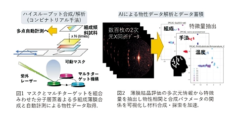
In addition to the combinatorial materials synthesis and evaluation technology (Figure 1), a high-speed thin-film materials synthesis technology that we have developed, the smart laboratory (SmartLab) is introducing materials informatics (MI), a multi-point analysis, database and computational science (Figure 2), to further accelerate materials development.
In device applications, the interface between different materials affects the properties and ease of synthesis. We have analyzed the chemical bonding and electronic structure of the interface using photoelectron spectroscopy and elucidated the band and defect structure. We have also elucidated the electronic and defect structures of various electronic material interfaces using in-situ observation techniques under device operating conditions.
Using these nanoscale interface characterization techniques, we will evaluate the fundamental device structures of materials obtained in the development of high-speed materials to verify device applications and solve problems.
Nano Electronics Device Materials Group | Research Center for Electronic and Optical Materials

Nano Electronics Device Materials Group
Group leader
Group members
AIM and GOAL
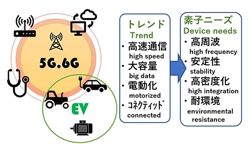
Nanoelectronics materials have been applied to various new devices for IoT, electric vehicle and so on. For these applications, demands of high reliability, high-speed operation, and high power are increasing.
Our group focuses on thin-film dielectric materials in electronic materials with the aim of developing new thin-film materials that contribute to high reliability and next-generation high-speed/high-power electronic devices.
Using combinatorial material development and interface evaluation techniques, we develop electronic materials that contribute to next-generation semiconductor devices such as film capacitors, memory devices, and high-k materials.
Our research targets
APPROACH
To accelerate the development of thin film materials, we are combining our combinatorial materials synthesis/evaluation technology with materials informatics. In addition, in the device application of new materials, the interfacial properties affect the physical and electrical properties.
We have elucidated the electronic and defect structures of various interfaces using in-situ observation techniques, in particular the application of voltage using photoelectron spectroscopy. We will verify and solve problems in the development of new materials and device applications through the collaboration of synthesis, evaluation, and data science.
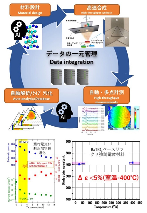
Overview of data-driven material development combined with combinatorial methods (top) and an example of achieving high-temperature stable high-dielectric thin films through additive optimization (bottom)
NAGATA, Takahiro / Group leader
Inorganic Thin Film Electronic Materials Development by Thin Film Materials Smart Lab
Overview
Electronic materials, such as semiconductors, are used in a wide range of applications in new technologies such as IoT and electric vehicles. In addition to high integration and multi-functionality, there is an increasing need for high durability, high-speed operation and ease of synthesis.
We focus on inorganic semiconductor/dielectric materials to develop new thin-film electronic materials that contribute to high reliability and next-generation high-speed/high-power electronic devices. Thin film dielectric materials have various applications such as capacitors, memory devices and insulating films, and we are promoting the introduction of informatics into materials design for each application. We are also working on the development of memory devices as an application of new materials, and aim to improve the functionality of the dielectric/semiconductor interface through the use of high-throughput materials development and interface evaluation techniques.
Characteristics
- Systematic exploration of thin film materials through high-throughput thin film synthesis and analysis technology
- Realization of thin film crystal growth condition search by physical property analysis using AI technology
- Complex oxide perovskite materials for high dielectric constant and high thermal stability materials
- Development of non-oxide high dielectric materials for non-oxide semiconductor materials
- Realization of high precision dielectric/semiconductor interface analysis and high functionality by combining photoelectron spectroscopy techniques
Major reserch 1
Major reserch 2
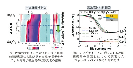
We have systematically analyzed the physical properties of oxide semiconductors, which are the next-generation materials for transistors and power devices, using combinatorial methods to address the problems of controlling carrier and surface electronic states, and have realized carrier control by solid solution and control of surface electron degenerate layer formation, which is a problem for device applications (Figure 3).
Based on the obtained data, we realized film formation condition search using MI-based data clustering and crystal layer control visualization by linking data from different synthesis methods (Figure 2).
Using the same method, we proposed an unconventional non-oxide high dielectric material for semiconductor devices (Figure 4) and improved the high dielectric constant and high temperature stability of dielectric materials for thin film capacitor applications.
Summary
The Thin Film Materials SmartLab accelerated the development of advanced thin film electronic materials and the search for new materials. Through systematic material synthesis and analysis, we have proposed the development of new materials for thin film dielectrics and improved the electronic properties and reliability of existing materials.
As expectations for thin-film electronic materials, especially semiconductors, continue to rise in response to accelerating societal needs for AI, DX, and electrification, our technology is expected to be applied to the development of next-generation semiconductors and functional thin-film materials.
YAGYU, Shinjiro
Development of an Automated Material Evaluation System
Overview
With the advancement of high-performance materials, a wide range of evaluations is required. At the same time, a comprehensive perspective is necessary to properly understand trade-offs in material properties.
To address this issue, in addition to specialized evaluation measurements related to high functionality, combining simple and diverse measuring devices is a potential solution. This study developed a material sequencer system that enables the integration of simple and diverse measuring devices by miniaturizing and modularizing each evaluation device while ensuring unified data acquisition across the entire system.
Furthermore, since large amounts of spectral data are generated through measurements, an automated analysis technology (including algorithms and implementation) has been developed. In particular, an algorithm was designed to automatically estimate the threshold of spectra that follow a power law.
Characteristics
- Development of an automated measurement system for fundamental properties (optical, electrical, and magnetic) in atmospheric conditions
- Miniaturization of a Kerr effect device for evaluating magnetic properties (soft and ferromagnetic)
- Development and implementation of an automated spectral analysis algorithm for power-law distributions
Major reserch 1
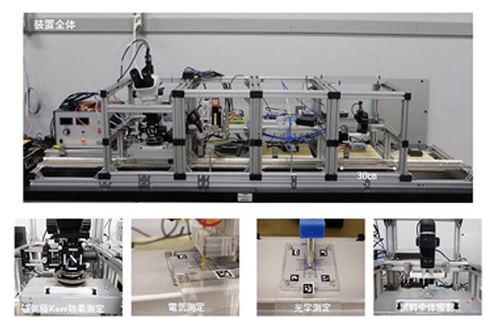
Simple Automated Material Evaluation System
A "Material Sequencer" was developed to automatically and continuously evaluate various inorganic materials. The image shows the external appearance of the device.
This system is designed as a "health checkup" for materials, allowing diverse evaluations using simple devices to provide an overview of high-performance materials. The evaluation data is collected and integrated with the assumption of machine learning analysis. Each measurement device is modularized, fitting within a 30 cm cube, with standardized input/output controls and sample access methods. The samples targeted are inorganic materials with a 0.5-inch size.
Currently, the system is capable of image measurement, reflection measurement, resistance measurement, and magnetic Kerr effect measurement. The magnetic Kerr effect device has been miniaturized using a pulse magnet to fit within this compact space.
Major reserch 2
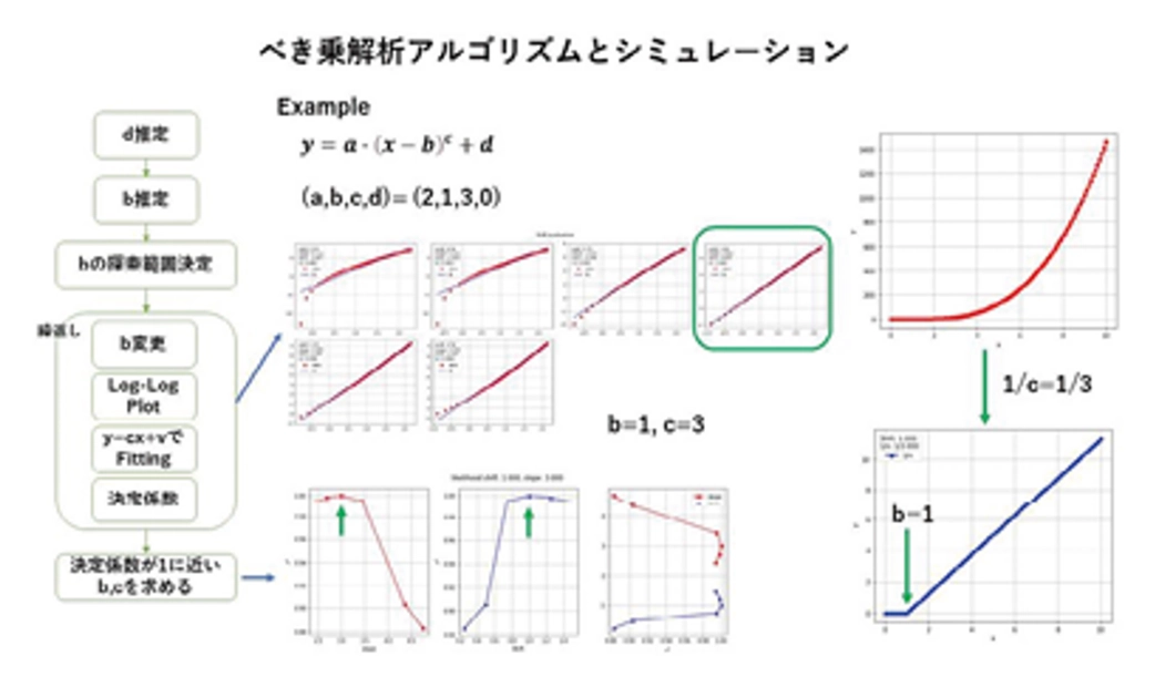
Automated Analysis of Spectra Interpretable by Power Law
Automated spectral analysis technology has been developed for physical phenomena. In spectral data interpreted by the power law, the threshold value and power exponent serve as parameters. Examples include the critical current density obtained from current-voltage measurements of superconducting materials, the bandgap from visible-ultraviolet absorbance, and the ionization potential from photoelectron yield spectroscopy.
The figure illustrates an algorithm for estimating the power exponent and threshold, along with its simulation. Power-law spectra are typically analyzed using double-logarithmic plots, but when the threshold shifts, a simple logarithmic transformation does not yield an accurate power exponent. Therefore, an adjusted plot incorporating the threshold shift is used for accurate estimation.
Additionally, if the power exponent is fixed for a given phenomenon, the threshold can be estimated using an extended ReLU function and an absolute error-based fitting method.
Summary
- Development of a system and a set of simple measurement devices for comprehensive material evaluation
- Development of a compact Kerr effect device using a pulse magnet for determining magnetic properties
- Development of an automated spectral analysis algorithm for power-law distributions
YAMASHITA, Yoshiyuki
physical properties of material discriminating points
Overview
Discriminating points in materials often determine the physical properties of materials. For examples, insulator/semiconductor interfaces, metal/semiconductor interfaces, defects, catalysts, and dopants in semiconductors are material discriminating points.
Since the density of discriminating points is very low generally, it is very difficult to elucidate their physical properties. Therefore, we have been studying discriminating points of the atomic structure and the chemical state using synchrotron-based X-ray absorption fine structural method and photoelectron holography.
we also have been investigating the physical properties of the discriminating points of the material using operando methods to accurately understand the physical properties of the discriminating points of materials.
Characteristics
- Physical properties of solid-solid interfaces by X-ray absorption and emission method
- Elucidation of atomic structures and chemical states of material discriminating points by photoelectron holography (eg. defects, catalytically active sites, active and inactive atoms of dopants, etc.)
- Elucidation of physical properties of material discriminating points by operando methods
Major reserch
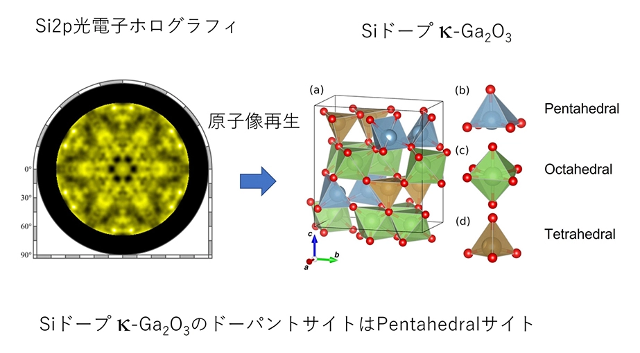
Though there are three inequivalent Ga sites in the Si-doped k-Ga2O3 unit cell, it is not clear which Ga site is replaced by a Si atom as a dopant. Photoelectron holography revealed that the substitution sites are mixture of three inequivalent Ga sites and the active Si dopant site is the tetrahedral substitution site.
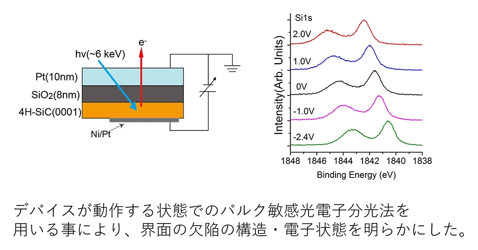
- Using operando bulk sensitive photoelectron spectroscopy, we revealed that electron occupation and occupation behavior in Pt/SiO2/4H-SiC based power devices. Combined with theoretical calculations, we clarified the atomic structures and the energy levels of interfacial defects at the SiO2/4H-SiC interface.
- Using X-ray absorption and emission spectroscopy, we clarified the site specific and the element specific valence band at the SiO2/Si interface. Based on the results, we reveled the site-specific dielectric constant at the vicinity of the interface.
1
2
Summary
We clarified the atomic structures and the chemical states of material discriminating points using photoelectron holography and X-ray absorption emission spectroscopy. We also revealed the dynamic properties of interface defects at solid-solid using operando photoelectron spectroscopy.
In the near future, we would like to efficiently reveal the physical properties of material discriminating points by introducing combinatorial methods.
Current Members (as of 2026)
Specially Appointed Research Fellow
YOSHITAKE, Michiko YOSHITAKE.Michiko@nims.go.jp
Postdoctoral Research Fellow
INDARI EfiDwi INDARI.EfiDwi@nims.go.jp
Graduate Research Assistant
WATANABE, Masaharu WATANABE.Masaharu@nims.go.jp
TOOSHIL Abul TOOSHIL.Abul@nims.go.jp
Project Technical Staff
NAKANE, Kazuaki NAKANE.Kazuaki@nims.go.jp
KONO, Takashi KONO.Takashi@nims.go.jp
KOBAYASHI, Tomoko KOBAYASHI.Tomoko@nims.go.jp
OGAWA, Ayako OGAWA.Ayako@nims.go.jp
KANIE, Minato KANIE.Minato@nims.go.jp
Temporary Staff(engineering)
MATSUSHITA, Michiyo MATSUSHITA.Michiyo@nims.go.jp

 Optical Single Crystals Group