Methods and technologies / Characterization and measurements | Research Center for Electronic and Optical Materials

Back to top

Methods and technologies
Characterization and measurements

The technologies used at this center can be broadly divided into synthesis/manufacturing technology and evaluation analysis technology.
This page focuses specifically on evaluation and measurement. Please see 【another page 】for Synthesis and processing methods.

There are also various ways to evaluate the obtained materials. Methods for investigating crystal and molecular structures, methods for evaluating electrical properties, methods for evaluating optical properties, and spectroscopic analysis for investigating electronic structures and lattice vibrations are also used. In addition, chemical evaluations such as catalytic properties and adsorption properties, as well as methods for investigating mechanical properties such as heat resistance and strength, are also used.

We also have equipment available for use by outside organizations. If you are interested, please inquire.

【Synthesis and processing】 page

Here, techniques for strctural analysis in this center will be introduced.

Scanning electron microscopy

We perform a variety of analyzes by combining scanning electron microscopes with various equipment such as spectrometers.

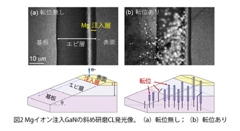
Evaluation of shape and defect structure using cathodoluminescence and electron beam induced current

Group in charge
Semiconductor Defect Design Group

CHEN, Jun

CL images of Mg-implanted GaN. Top: 10 micrometer micrographs comparing a dark area without dislocations to an area with white spots. Bottom: schematics show an electron beam scanning the beveled substrate, epitaxial, and Mg layers, illustrating how light is emitted at dislocation sites.

Transmission electron microscopy

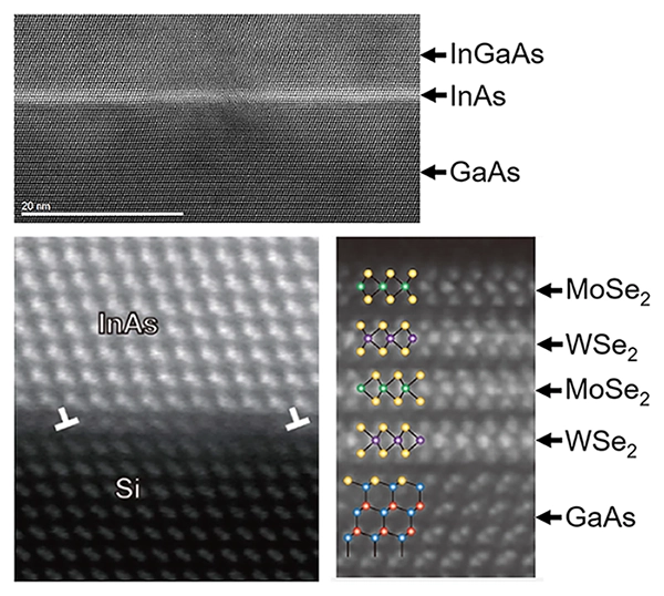
Transmission electron microscopy is used for various structural evaluations such as nano-sized structures and crystal defects.

Three high-resolution TEM images. Top: 20 nm scale cross-section of GaAs and InAs layers. Bottom left: InAs on Si, with two interface dislocations marked by T-symbols. Bottom right: atomic arrangement of alternating WSe2 and MoSe2 layers on GaAs, with crystal structure models showing precise stacking.

Probe microscopes

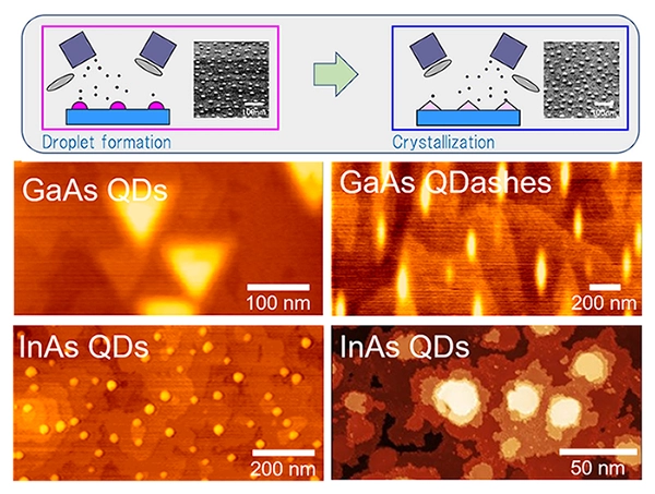
Atomic force microscopy (AFM) is used to evaluate nano-sized surface.

AFM image 'Figure 3' of a semiconductor surface. Parallel diagonal stripes show atomic steps or terraces just one atomic layer high. This demonstrates an extremely smooth crystal surface, precisely controlled at the atomic level, highlighting the excellence of the thin-film growth process. Nanostructure fabrication via droplet epitaxy. Top: schematic of droplet formation to crystallization. Bottom: four microscopy images showing triangular and elongated Gallium Arsenide structures, and Indium Arsenide dots at scales from fifty to two hundred nanometers. It demonstrates diverse shape control.

X-ray diffraction

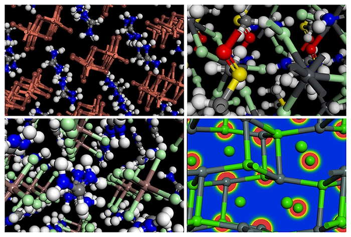
It is used not only to determine crystal structure, but also to evaluate various structures such as thin film thickness and particle size.

Four simulations of hybrid crystal structures. Three images show intricate networks of carbon and nitrogen atoms. The bottom right visualizes electron density, with red and yellow contours around green atoms on a blue background, predicting chemical bonding and charge distribution at an atomic level.

Electron beam diffraction

We utilize various electron beam diffraction techniques such as transmission electron microscopy, RHEED, and LEED to identify crystal structures and surface structures.

By analyzing the emission direction of photoelectrons observed using X-ray photoelectron spectroscopy or ultraviolet photoelectron spectroscopy (photoelectron diffraction method), it is also possible to identify the atomic arrangement on the top-most surface and sub-surface

Group in charge
Nano Electronics Device Materials Group

YAMASHITA, Yoshiyuki

Si 2p photoelectron holography. Left: reconstructed yellow atomic image. Right: crystal models of Si-doped kappa-Ga2O3. The analysis identifies the five-fold coordinated Pentahedral site as the stable dopant position among the three Pentahedral, Octahedral, and Tetrahedral site candidates.

We will introduce state analysis and composition analysis at this center.

Electron spectroscopy

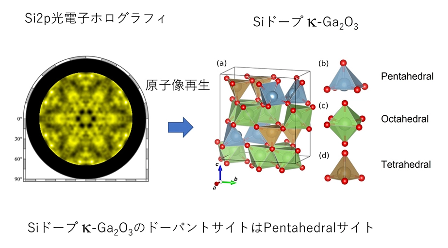
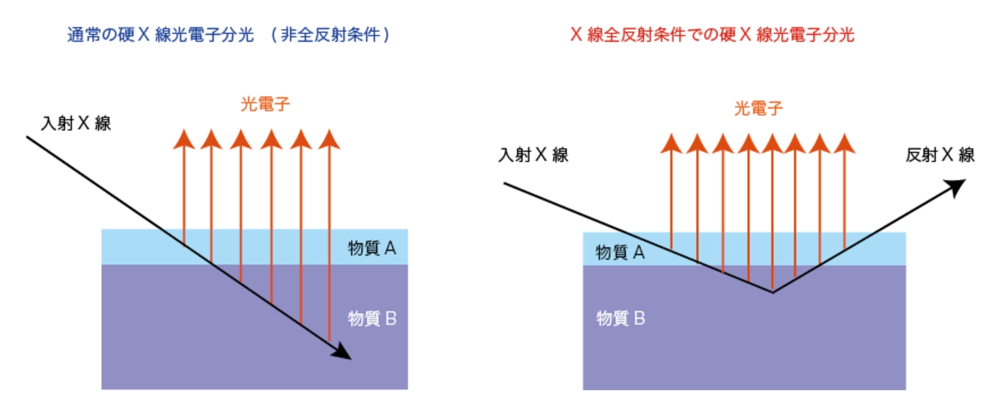
In particular, we utilize photoelectron spectroscopy, including hard X-ray photoelectron spectroscopy, to evaluate the chemical composition and electronic structure of substances and materials.

Hard x-ray photoelectron spectroscopy

Group in charge
Electro-ceramics group

UEDA, Shigenori

Hard X-ray Photoelectron Spectroscopy. Left: non-total reflection where X-rays penetrate Material A and B for bulk observation. Right: total reflection at a grazing angle, reflecting at the A/B interface for selective interface observation, demonstrating control over the probe depth in HAXPES.

Evaluation of crystal defect states

Development of evaluation device: Photothermal deflection spectroscopy

Group in charge
Electro-ceramics Group

SUMIYA, Masatomo

Nitride semiconductor research. Center: cross-section of a Gallium Nitride High Electron Mobility Transistor. Around it are an MOCVD system photo and three graphs: current-voltage, photothermal deflection spectroscopy, and magneto-resistance, depicting a cycle from growth to device evaluation.

Evaluation using isotope tracer

Group in charge
Electro-ceramics group

Arrhenius plot of 18O dependence in La2O3. Vertical axis: diffusion coefficient; horizontal: reciprocal temperature. Compared to dashed CeO2, this study shows a linear decrease from 10 to the -9th to -12th as reciprocal temperature increases from 10 to 15, indicated by red squares and a solid line.

cathodoluminescence

Group in charge
Semiconductor Defect Design Group

CHEN, Jun

Bevel polishing for semiconductor layers. Left: stacked block and shallow cut. Right: polishing at a small angle like 3 degrees expands nanometer-thick layers to micrometer widths on the surface, increasing spatial resolution in the thickness direction by about 20 times for detailed observation.

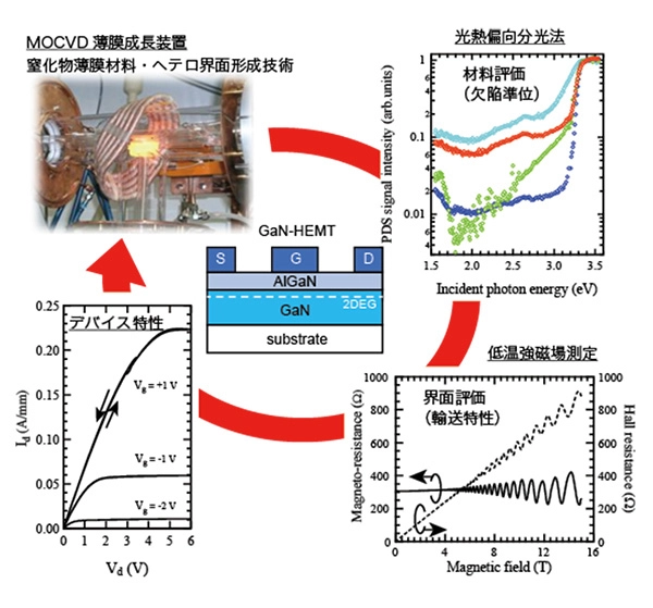
We would like to introduce the property evaluation techniques at this center.

Installation of physical property evaluation method

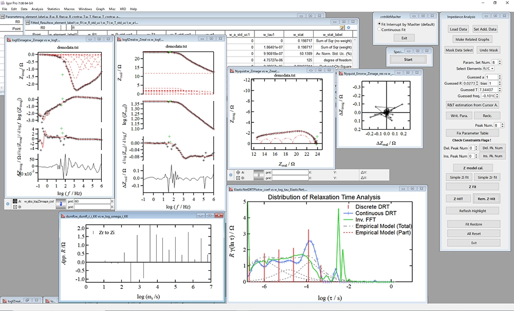
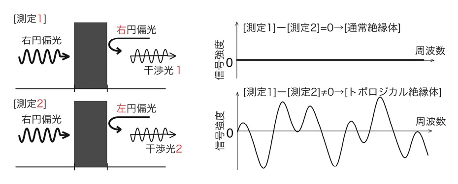
We are developing and implementing property evaluation equipment necessary for material development, such as new measurement equipment that captures quantum phenomena.

Development of equipment for quantum optical measurements

Group in charge
Quantum Photonics Group

KURODA, Takashi

Quantum optics setup and data. Right: optical breadboard apparatus. Left: three graphs at 7, 25, and 80 nW. All show a sharp dip at zero nanoseconds, visually proving the single-photon emission property where photons are generated one by one, a key result for quantum light sources.

ODMR, opticaly detected magnetic resonance

Group in charge
Semiconductor Defect Design Group

TERAJI, TokuyukiWATANABE, Kenji

Close-up of an optical measurement setup. A bright green laser beam passes through multiple lens holders on a black breadboard, focusing on a single point on a small component. This illustrates the precise path and focusing of light for device evaluation and measurement experiments.

Application of data science

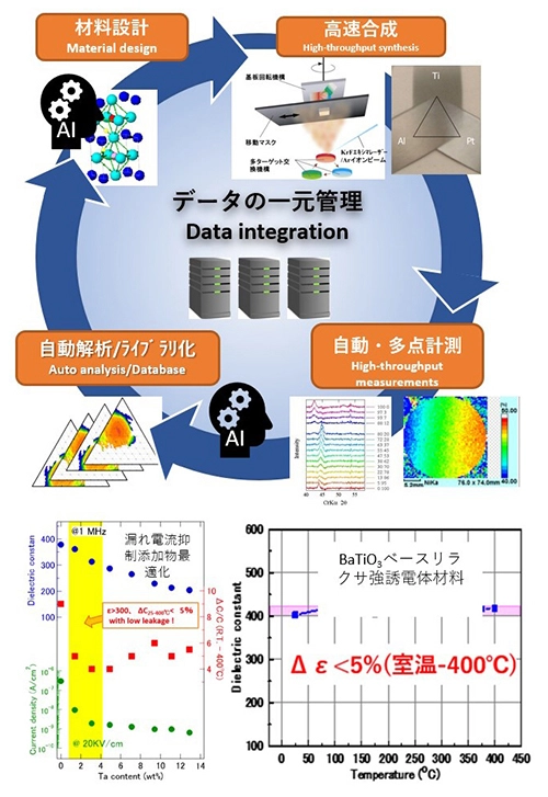
We are proceeding with efforts to automate and make our equipment autonomous, with the aim of speeding up substance searches, avoiding missing data and human-related variations, and creating libraries for data utilization.

Development of automatic measurement system

Group in charge
Nano Electronics Device Materials Group

YAGYU, Shinjiro

Power-law analysis. Left: Flowchart to find parameters where the coefficient of determination is near 1. Center top: Formula y equals a times (x minus b) to the c, plus d. Right: Simulation shows a red power-law curve linearized into a blue line starting at b, using a calculation of 1 divided by c.

Building a combinatorial smart lab system

Group in charge
Nano Electronics Device Materials Group

NAGATA, Takahiro

AI-driven material development. Top: Circular workflow of design, high-throughput synthesis, measurement, and analysis with data integration. Bottom: Property graphs of a BaTiO3-based relaxor ferroelectric, showing high thermal stability with less than 5% dielectric constant variation from RT up to 400°C.

Introducing calculations and analysis at this center.

Analysis program development

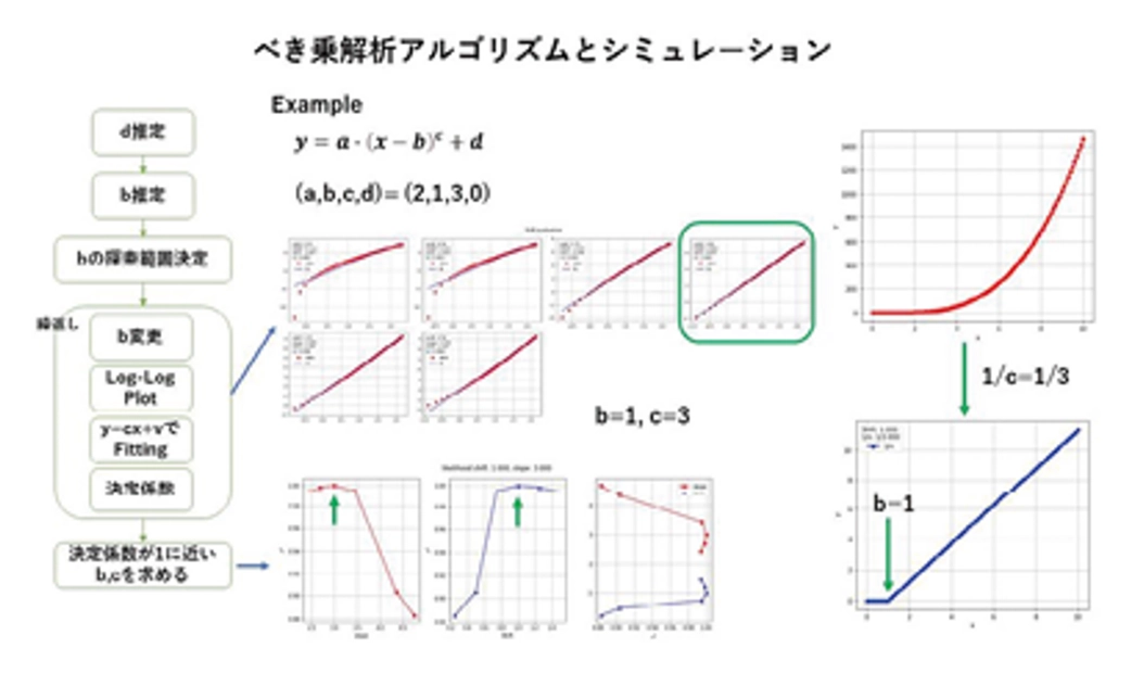
We are developing programs necessary for evaluator analysis of material properties.

Impedance analysis program

Group in charge
Optical Ceramics Group

KOBAYASHI, Kiyoshi

Operation screen of 'Igor Pro' for impedance analysis. Multiple windows show Nyquist plots and relaxation time distribution graphs. Each features measured data with red calculated fitting curves. On the right, a control panel with buttons like 'Z Fit' is arranged for electrochemical data analysis.

Automatic spectrum analysis program

Group in charge
Nano Electronics Device Materials Group

YAGYU, Shinjiro

Power-law analysis. Left: Flowchart to find parameters where the coefficient of determination is near 1. Center top: Formula y equals a times (x minus b) to the c, plus d. Right: Simulation shows a red power-law curve linearized into a blue line starting at b, using a calculation of 1 divided by c.

Theory construction

Search for unique nanophotonics functions

Group in charge
Quantum Photonics Group

OCHIAI, Tetsuyuki

Potential distribution on a sphere. Bottom: 3D model with surface potential in purple-to-yellow gradient. Top: Graph of potential versus distance. Sharp fluctuations at boundaries minus 1 and plus 1 indicate a specific electrical response near the surface, illustrating light-matter interaction.

Mathematical material theory

Group in charge
Semiconductor Defect Design Group

INOUE, Junichi

Material identification via light reflection. Left: Schematics of Measurements 1 and 2 using circularly polarized light. Right: Graphs showing a Normal Insulator (1 minus 2 equals 0) and a Topological Insulator (non-zero wave), illustrating how light reflection identifies topological properties.

Molecular/crystal simulation

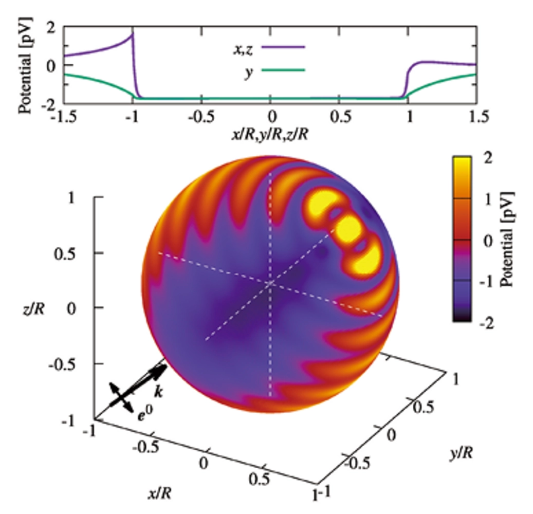
In order to gain a deep understanding of materials, we conduct electronic state calculations based on quantum mechanics and atomic arrangement simulations based on them.

Consideration of natural minerals, nanosheets, etc

Group in charge
Environmental Circulation Composite Materials Group

SUEHARA, Shigeru

Nanomaterials. A: Ions between mica layers reacting with water. B: Atomic arrangement and energy band of a new sheet, showing a Dirac cone. C: Schematic of ions passing through a mesh framework. Each panel illustrates how atomic structures define the material's physical properties and functions.

Search for semiconductors and dielectrics

Group in charge
Electro-ceramics group

OHASHI, Naoki

Four simulations of hybrid crystal structures. Three images show intricate networks of carbon and nitrogen atoms. The bottom right visualizes electron density, with red and yellow contours around green atoms on a blue background, predicting chemical bonding and charge distribution at an atomic level.
Research Center for Electronic and Optical Materials SITE MAP