Crystal growth and device fabrication of
wide bandgap oxides such as gallium oxide
Group in charge
Ultra-wide Bandgap Semiconductors Group
OSHIMA, YuichiOSHIMA, Takayoshi

At this center, we are conducting research and development on a wide variety of substances in order to acquire the desired material technology.
First, semiconductors are a typical functional material. Semiconductors are also used as switches that control current by utilizing their electron transport properties, and as chemical sensors that identify substances. Semiconductors are also used for light emitting and light receiving, that is, in devices that emit various types of light, such as lighting and displays, as well as in light sensors and solar cells.Materials that emit light include fluorescent materials, which are materials with a light-emitting structure built into them, and optical materials, such as lenses. In addition, there is a method of imparting fine structure to materials to achieve optical and electronic functions. A typical example is nanostructures such as metamaterials, which can be called nanosized antennas.Additionally, the materials needed for electronics include insulating materials such as capacitors, packaging materials, and piezoelectric materials. Additionally, some substances perform chemical functions such as trapping molecules or transporting ions.
At this center, material development is progressing from a variety of perspectives, from the search for new substances that exhibit unprecedented high functionality to technologies for applying superior materials as devices.
We would like to introduce the research and development of semiconductors at this center, especially semiconductors focusing on electron transport.
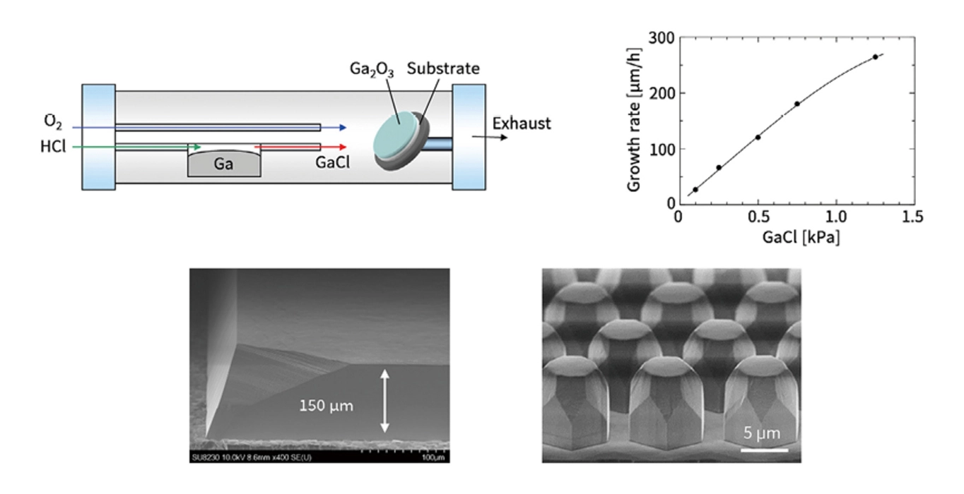
We are developing wide band gap semiconductors for high voltage power control.
Group in charge
Ultra-wide Bandgap Semiconductors Group
OSHIMA, YuichiOSHIMA, Takayoshi
Group in charge
Ultra-wide Bandgap Semiconductors Group
KOIZUMI, Satoshi
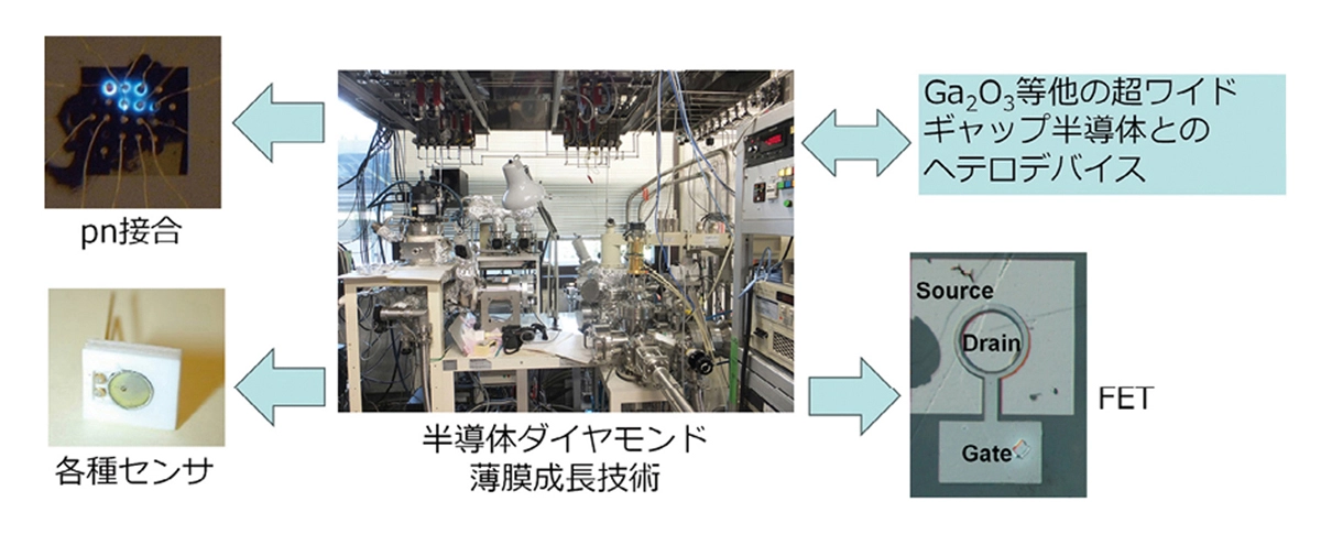
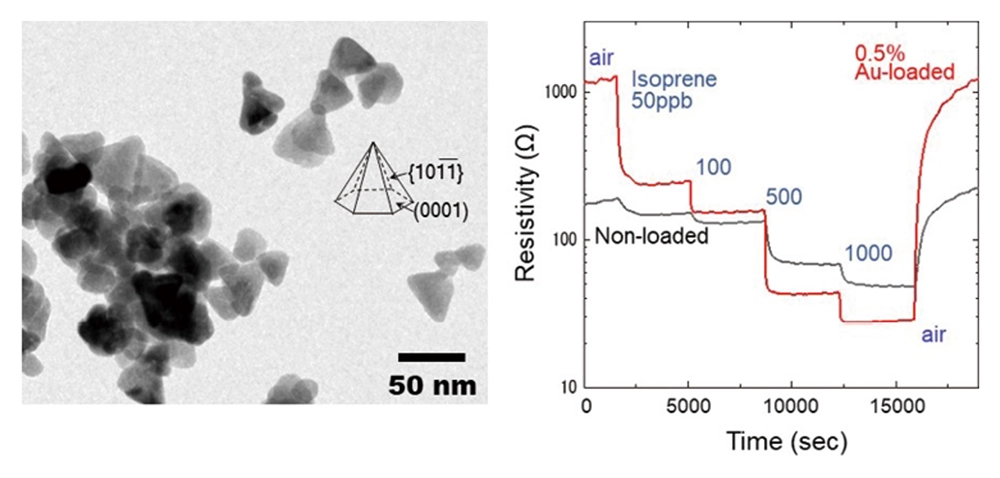
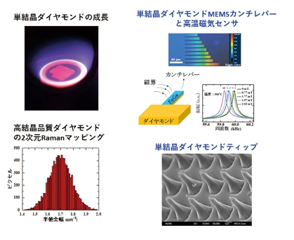
We are developing sensor semiconductors that utilize the chemical activity of semiconductor surfaces.
Group in charge
Electro-ceramics Group
ADACHI, YutalaSAITO, Noriko
Group in charge
Ultra-wide Bandgap Semiconductors Group
IROKAWA, Yoshihiro
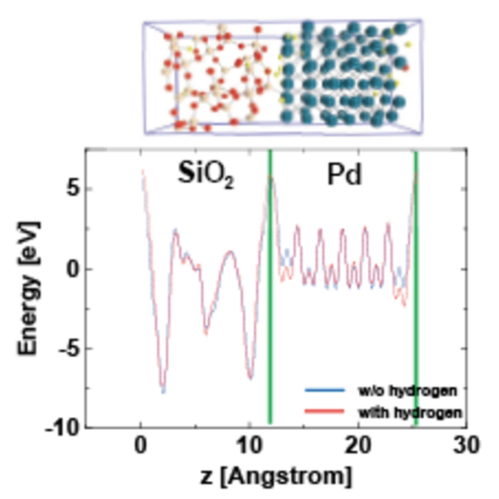
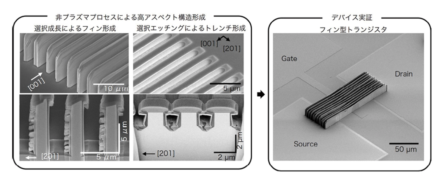
We are developing materials and forming bonds to improve the functionality of electronic devices such as transistors.
Group in charge
Electro-ceramics Group
OHSAWA, Takeo

Group in charge
Semiconductor Defect Design Group
LIU, Jiangwei
The appearance of new materials can change the industrial structure. We are currently searching for semiconductors with properties such as high mobility.
Group in charge
Amorphous Material Group
OGAKI, Takeshi
Group in charge
Electro-ceramics Group
SUEHIRO, Takayuki
We would like to introduce the research and development of semiconductors at this center, with a particular focus on semiconductor applications related to light.
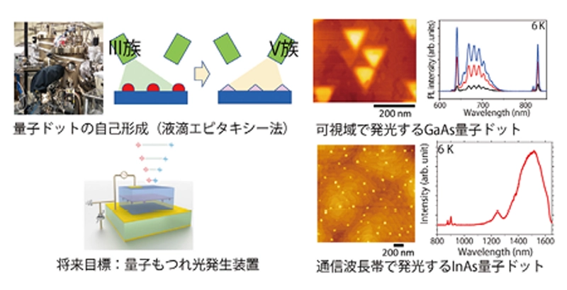
We are working on compound semiconductor materials and their nanostructure control with the aim of developing highly efficient light emission and highly sensitive optical sensors.
Group in charge
Semiconductor Epitaxial Structures Group
MANO, Takaaki
OHTAKE, Akihiro
KAWAZU, Takuya
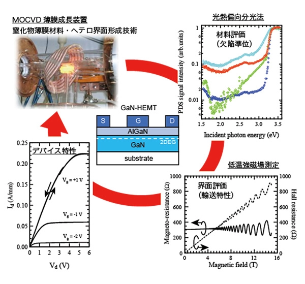
We are working on developing III-V nitride semiconductors, from aluminum nitride to indium nitride, with the aim of increasing their functionality.
Group in charge
Electro-ceramics Group
SUMIYA, Masatomo
Group in charge
Semiconductor Epitaxial Structures Group
IMURA, Masataka
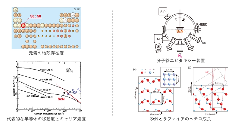
We are currently exploring new semiconductors that are not classified as III-V or II-VI, especially direct transition type semiconductors.
Group in charge
Electro-ceramics Group
OHASHI, Naoki
SAITO, Noriko
Group in charge
Electro-ceramics Group
OHASHI, NaokiIMAI, Motoharu
We would like to introduce the research and development of phosphors and optical materials at this center.
We are conducting research and development aimed at reducing the power consumption of lighting, improving display quality, and improving the functionality of phosphors in the infrared region.
Group in charge
Advanced Phosphor Group
TAKEDA, Takashi

Group in charge
Advanced Phosphor Group
NAKANISHI, Hiroyuki

Group in charge
Optical Single Crystals Group
SHIMAMURA, KiyoshiVILLORA, Garcia
We are developing ceramic laser materials for high-power lasers such as industrial lasers.
Group in charge
Optical Ceramics Group
SUZUKI, TohruFURUSE, Hiroaki
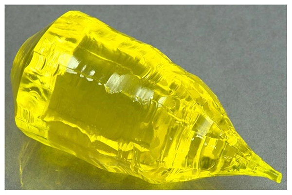
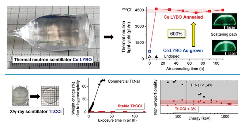
We are developing scintillator materials for radiation detection, which are important in security and medical fields.
Group in charge
Optical Single Crystals Group
SHIMAMURA, Kiyoshi
Group in charge
Polycrystalline Optical Material Group
MORITA, Koji
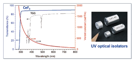
We are developing electro-optical and magneto-optical materials used for wavelength conversion and polarization control.
Group in charge
Optical Single Crystals Group
SHIMAMURA, KiyoshiVILLORA, Garcia
Group in charge
Quantum Photonics Group
KURIMURA, Sunao

Group in charge
Nanophotonics Group
FUDOUZI, Hiroshi

Group in charge
Semiconductor Epitaxial Structures Group
MIYAZAKI, Hideki
Group in charge
Nanophotonics Group
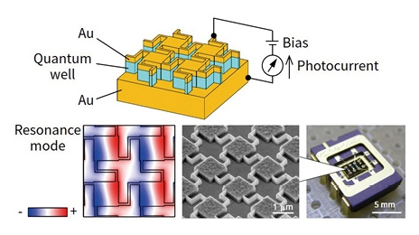
IWANAGA, Masanobu
We would like to introduce the research and development of nanostructures and composite materials at this center.
We are developing photonic devices adopting microfabrication and nanomaterial synthesis.
Group in charge
Semiconductor Epitaxial Structures Group
MIYAZAKI, Hideki
Group in charge
Nanophotonics Group
IWANAGA, Masanobu

Group in charge
Semiconductor Epitaxial Structures Group
MANO, TakaakiOHTAKE, AkihiroKAWAZU, Takuya
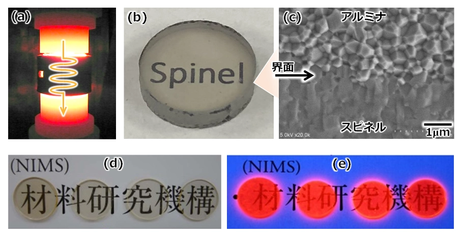
We are proceeding with the development of nanopowder as a raw material for making ceramics and to obtain the advantage of high specific surface area.
Group in charge
Polycrystalline Optical Material Group
LI, Jiguang

Group in charge
Electroceramics Group
SAITO, Noriko
We are developing nanocomposites with the aim of creating high-strength substrates and materials with controlled heat conduction.
Group in charge
Polycrystalline Optical Material Group
VASYLKIV, Oleg

Group in charge
Optical Ceramics Group
ESTILI, Mehdi
We would like to introduce the research and development of dielectrics and piezoelectrics at this center.
We are developing dielectrics and piezoelectrics for various applications such as electronics, sensors, and actuators.
Group in charge
Electro-ceramics Group
SHIMIZU, Takao
Group in charge
Nanophotonics Group
IWANAGA, Masanobu

Group in charge
Nano Electronics Device Materials Group
NAGATA, Takahiro
We are developing materials for the further development of MEMS, such as frequency filters and magnetic sensors.
Group in charge
Ultra-wide Bandgap Semiconductors Group
LIAO, Meiyong
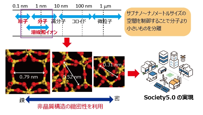
We are investigating amorphous materials without grain boundaries not only as optical materials but also as insulators and dielectrics.
Group in charge
Amorphous Material Group
SEGAWA, Hiroyo
We would like to introduce the research and development of chemically functional materials such as ionic conductors and adsorption materials at this center.
We are developing hydrogen ion conductors for energy applications such as fuel cells.
Group in charge
Environmental Circulation Composite Materials Group
KIM, JedeokTAMURA, Kenji

We are developing materials with low environmental impact that utilize biopolymers and natural resources.
Group in charge
Environmental Circulation Composite Materials Group
TAMURA, Kenji

Group in charge
Environmental Circulation Composite Materials Group
TAMURA, KenjiSAKUMA, HiroshiSUEHARA, Shigeru

Group in charge
Amorphous Material Group
SEGAWA, Hiroyo
Group in charge
Electro-ceramics Group
OHASHI, Naoki
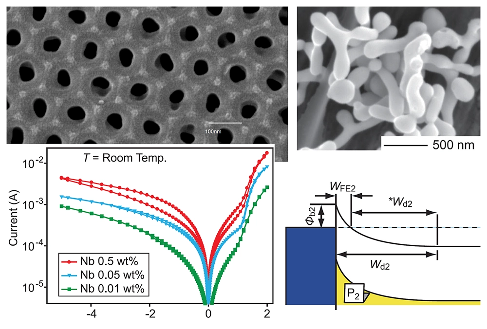
We are developing sensor materials that utilize the chemical activity of semiconductor surfaces.
Group in charge
Electro-ceramics Group
ADACHI, YutalaSAITO, Noriko

We would like to introduce the research and development conducted at our center regarding the exploration of the substances and functions of amorphous materials.
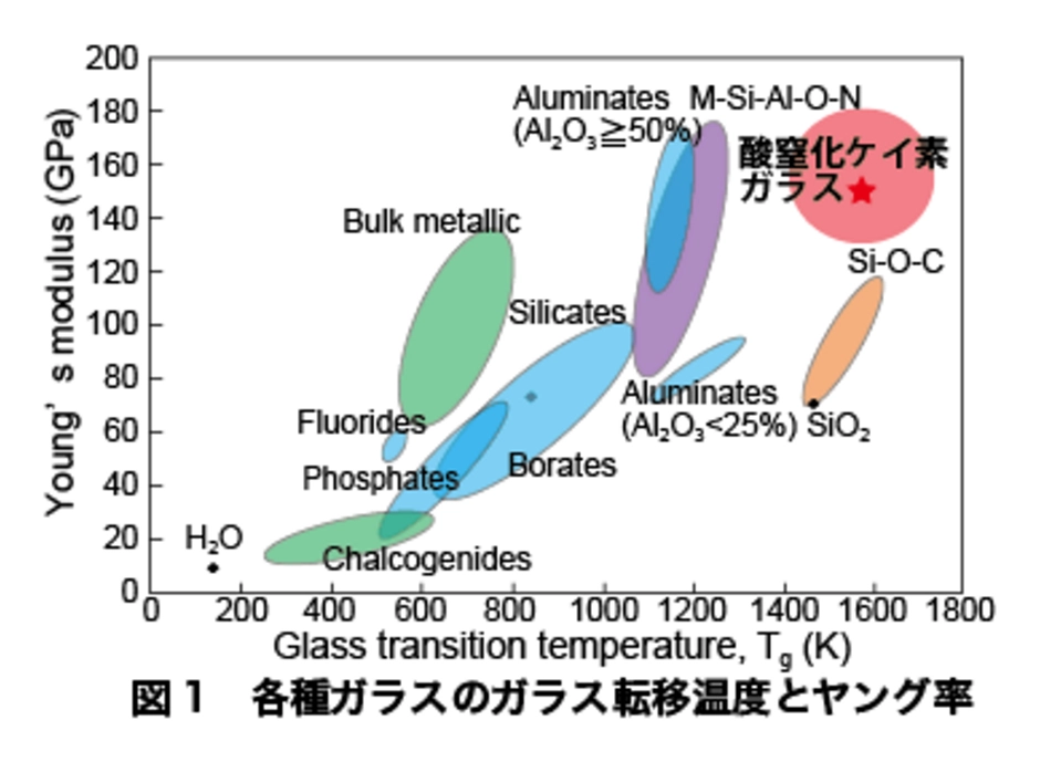
We are developing mixed anionic glass materials containing oxygen and nitrogen to improve the heat resistance, chemical durability, and optical properties of glass.
Group in charge
Amorphous Material Group
SEGAWA, Hiroyo