 TERAJI.Tokuyuki@nims.go.jp
- NV center formation:
Nitrogen-doped diamonds of various concentrations are grown using chemical vapor deposition (CVD) and high temperature and high pressure synthesis (HPHT) methods, and heat treated in various environments. - Spin characterization:
Spin properties of diamond crystals are evaluated using pulsed optical-domagnetic resonance spectroscopy (ODMR). Multiple spectroscopic evaluations such as confocal PL, ESR, and FTIR will be used to further evaluate a variety of crystals to accurately determine the quantum properties of the crystals. - Construction of NV center formation science:
From steps (1) and (2), we will determine the type and concentration of point defects formed in diamond crystals and quantitatively investigate the effect of these defects on the spin properties of NV centers. Based on the results of step (3), the diamond crystal growth conditions are reconsidered and diamond growth under new conditions is carried out.
Semiconductor Defect Design Group | Research Center for Electronic and Optical Materials

Semiconductor Defect Design Group
Group leader
Group members
AIM and GOAL
- Defect control of semiconductors not only leads to the creation of high-quality materials, but also to the discovery of new functions using defects. For example, the designed defects in diamond will enable new devices for applications such as quantum bits and quantum sensing.
- The Semiconductor Defect Design Group is focusing on wide bandgap semiconductor materials. We aim to realize technologies with high social value, such as applying room-temperature quantum technology, improving energy efficiency, and reducing environmental impact.
APPROACH
- Growth Process:
Defect control involves many factors, including the growth process and material composition. We are working to create higher quality semiconductor materials by optimizing the growth process and controlling impurities densely. - Defect characteristics:
We gain knowledge for controlling defect formation by characterizing optical and electrical properties of defects. Aiming at quantum properties good to use, we incorporate methods of condensed matter theory and quantum optics, and construct an effective framework focusing on essentials of phenomena.
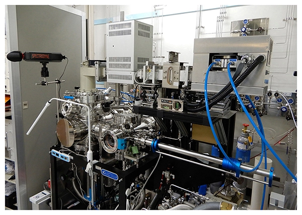
FIG 1 Chemical vapor deposition system for growing high-purity diamond single crystals
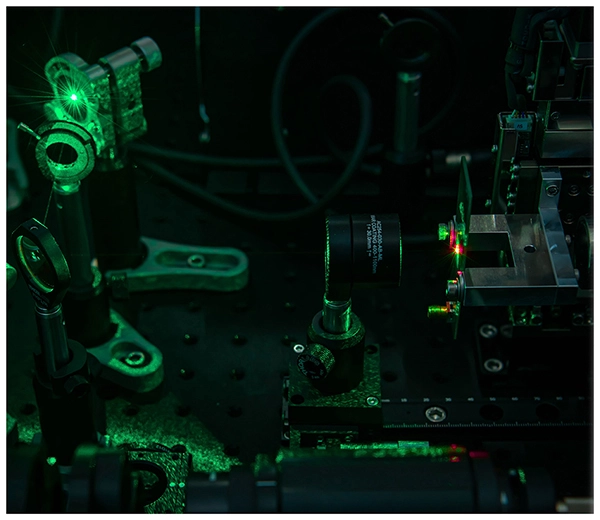
FIG 2 Optically detected magnetic resonance (ODMR) system for characterizing quantum properties (red fluorescence light reflecting is emitted from diamond)
TERAJI, Tokuyuki / Group Leader
Diamond Crystal Growth and Quantum Device Applications
Overview
For practical application of quantum magnetic sensors using diamond NV centers, further improvement of sensitivity is essential. We have been studying to improve the quantum properties of NV centers formed in diamond crystals by enhancing the diamond crystal growth technique, thereby increasing the sensitivity of magnetic sensors.
In particular, we are focusing on precise control of the concentration of NV centers and nitrogen in the crystal, reduction of impurities and defects that shorten the spin coherence time T2 (the time to hold the spin state; a longer T2 is necessary for higher sensitivity) of NV centers, and control of the spatial arrangement of NV centers on a nanoscale, The research is currently focused on increasing the crystal size.
Characteristics
- Advanced diamond crystal growth technology for quantum applications
- Research infrastructure that enables seamless implementation of crystal growth, quantum and optical characterization, and point defect structure identification
- Precise control of nitrogen concentration to improve quantum sensor sensitivity
- Large diamond crystals grown by CVD method
- Isotope control of 12C diamond crystals, etc.
Major reserch
Our research strategy to prepare diamond crystals for quantum sensing is illustrated in the figure.
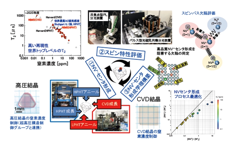
By implementing crystal growth, quantum and optical characterization, and point defect structure identification seamlessly in this way, the spin properties of NV centers can be reliably improved.
Summary
Many institutes around the world are currently working intensively to improve the sensitivity of quantum sensors. Most of activities are focused on the measurement method, while “advanced fabrication of NV centers in diamond crystals,” which has the greatest impact on sensitivity improvement, is difficult and is performed by only a limited number of institutes worldwide.
At NIMS, a team consisting of researchers from CVD growth, HPHT growth, quantum and optical characterization, and computation/theory has been working on this difficult task from various a perspectives and in a comprehensive manner.
This research framework has steadily improved the properties of diamond NV centers. In the future, we plan to conduct research focusing on spin defects other than diamond NV centers.
WATANABE, Kenji
CVD synthesis of hexagonal boron nitride
Overview
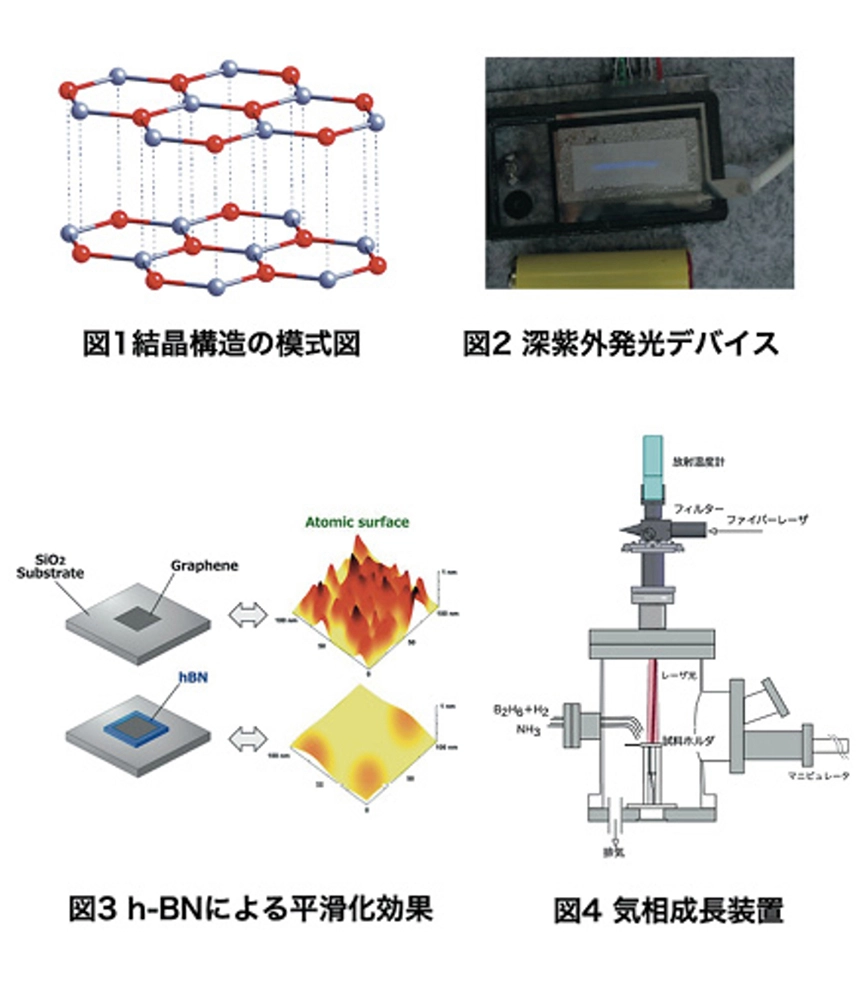
Hexagonal boron nitride (hBN) is a compound with a graphite-like crystal structure composed of nitrogen and boron (Fig. 1). It is commonly used as a heat insulating material and an electrical insulator due to its excellent chemical and thermal stability. Additionally, its mechanical properties make it an effective lubricant. However, before our research, there were no examples of the synthesis of high-purity single crystals, and their application as electronic materials was completely unknown.
We have successfully synthesized high-purity single crystals using the high-pressure method and investigated their optical properties. This has led to significant achievements, including the development of new ultraviolet light-emitting materials and contributions to two-dimensional atomic layer science.
We are currently working to further advance this research by synthesizing high-purity single crystals using a versatile vapor deposition method. These high-purity single crystals are crucial as materials for next-generation device applications, and our efforts are ongoing.
Characteristics
- Hexagonal boron nitride is a durable wide bandgap material with excellent chemical and thermal stability.
- It emits high-efficiency excitonic emission in the deep ultraviolet region (215 nm) and is considered for use in light-emitting devices to replace mercury lamps.
- It is a graphite-like layered compound that is essential for two-dimensional atomic layer science research focused on forming and protecting atomic layer planes.
- As a basic technology development for next-generation device applications, we aim to establish a technology for growing high-purity, low-defect crystals using a versatile vapor phase deposition method.
Major reserch
The maximum luminous intensity of high-purity hexagonal boron nitride (hBN) single crystals at room temperature, produced by the high-pressure, high-temperature method, is achieved at a wavelength of 215 nm (with an internal quantum efficiency of about 5% or more). A prototype device using an accelerated electron beam as the excitation source showed light intensity of about 8 µW/cm²/nm (Fig. 2). This emission wavelength region, known as the Far UV-C region, is considered safe even with ultraviolet light sources, as it cannot penetrate the human skin while still having a germicidal effect on bacteria and viruses.
On the other hand, using hBN single crystal as a substrate for two-dimensional atomic layer materials, such as graphene, can minimize surface potential fluctuations. The schematic diagram in FIG. 3 illustrates the fluctuation of surface potential and surface roughness when hBN is used as a substrate (lower row). Compared to graphene on an SiO₂ substrate (upper row), which was used in the early stages of graphene research, the surface uniformity is significantly higher. Due to this property, hBN has become known as an indispensable material for two-dimensional atomic layer devices.
In this research, we are working on the development of basic technologies to realize the characteristics of hBN through vapor phase deposition, which has a wider range of applications. As shown in FIG. 4, diborane and ammonia gas are used as sources for Group III and V atoms, respectively, and crystal growth is performed on a laser-heated substrate. By optimizing the substrate, temperature, and growth atmosphere control, we aim to grow thin films with higher purity and fewer defects.
Summary
hBN is a layered compound and is expected to pave the way for a variety of device applications by combining it with two-dimensional materials like graphene. hBN itself is a very anisotropic material, and new properties (emission, optical nonlinearity, and crystal symmetry control) have been reported. Implementing a more versatile vapor deposition method is essential for new breakthroughs in 2D material applications in the future.
CHEN, Jun
Cathodoluminescence characterization of Mg ion implanted GaN
Overview
Gallium nitride (GaN) materials are attracting attention as semiconductors for power devices that will be the key to energy saving, and are an important research topic in the future of the semiconductor industry. The key to the manufacturing technology is the production technology for p-type GaN using Mg ion implantation. Although various analysis methods have been used to evaluate defects in the vicinity of the wafer surface, there has been no method for visualizing the spatial distribution of activated Mg atoms, and this has been a major obstacle to improving productivity during mass production of GaN devices.
We addressed this issue using cathodoluminescence (CL) combined with a scanning electron microscope (SEM) and a spectrometer.
Characteristics
- The thickness of the ion implantation layer is less than 1 µm, and it is difficult to resolve in the depth direction using traditional CL with the spatial resolution limited to 100 nm
- We proposed a high-depth-resolution CL method using angle-cutting, and increased the depth resolution to about 10 nm
- With advances in sample preparation technology, it is applicable to the analysis of multilayer films and nano-structures
Major reserch 1
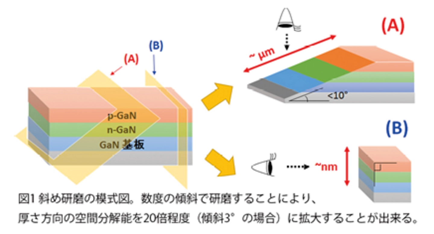
As shown in Figure 1, by cutting the sample at an angle of a few degrees, the spatial resolution in the thickness direction can be improved by about 20 times (for an inclination angle of 3°).
By measuring the line profile of the CL spectrum of the angle-cutting sample, we investigated the characteristic changes in the vicinity of the Mg ion implantation layer. Among the improvements made to the device manufacturing process, we have developed a CL observation method using low-energy electron beams with angle-cutting samples.
Using this method, we were able to clarify the electrical activation and depth distribution of Mg in Mg-ion-implanted GaN layers, as well as the relationship between Mg diffusion and threading dislocations. We hope to apply this method to various devices and expand our evaluation to other semiconductor wafers and substrates.
Major reserch 2
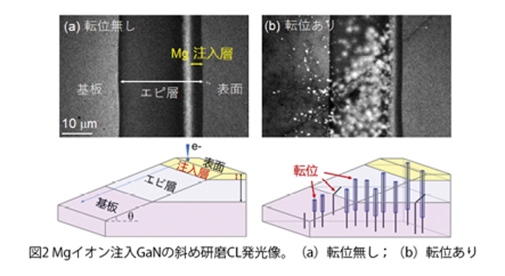
Figure 2 shows the CL images of an angle-cutting sample with a Mg implantation layer/n-GaN/GaN substrate structure at 3.28 eV, which is the characteristic donor-acceptor pair (DAP) emission associated with the activated Mg.
(a) shows an area without dislocations, while (b) shows another area with a high density of dislocations. The DAP emission from the Mg-implanted layer is weak indicating that the implantation process needs to be further improved. When dislocations are present, the dislocations become brighter and the DAP luminescence becomes stronger, indicating that Mg pipe diffusion via dislocation is occurring.
Summary
Among the improvements made to the device manufacturing process, we have developed a high-depth-resolution CL observation technique using low-energy electron beams and angle-cutting samples. Using this technique, we have been able to clarify the electrical activation and depth distribution of Mg in Mg ion-implanted GaN layers, and the Mg diffusion via dislocations. We hope to apply this technique to various devices and expand our evaluation to other semiconductor wafers and substrates.
LIU, Jiangwei
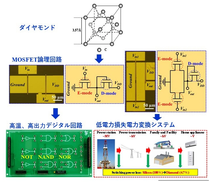
Diamond MOSFET Logic Circuits
Overview
Diamond is expected to be applied to power switches and integrated circuits that operate stably at high temperatures, high power, and high frequencies due to its high carrier mobility, large breakdown field, and high thermal conductivity.
As the first step towards developing diamond integrated circuits for extreme environments, we have successfully developed diamond logic circuits combining metal-oxide-semiconductor field-effect transistors (MOSFETs) with normally-on/off operation modes.
Characteristics
- Development of diamond MOS capacitors with extremely low leakage current density
- Development of control processing for normally-on/off operation of diamond MOSFETs
- Development of diamond MOSFET logic circuits
- Development of diamond power conversion systems with high thermal stability and low power loss
- Development of high-current output multi-gate diamond MOSFETs
Major reserch
In 2012, the interfacial band configurations of various oxides on hydrogen-terminated diamond (H-diamond) were determined using photoelectron spectroscopy technique. It was concluded that the large band offset energy at the Al2O3/H-diamond interface is advantageous for high-performance MOS electronic devices.
In 2013, the H-diamond MOS capacitors with extremely low leakage current density were achieved, along with the challenging development of normally-off H-diamond MOSFETs.
In 2014, NOT logic circuits were fabricated using H-diamond MOSFETs and load resistors. In 2015, control processing for fabricating normally-on/off H-diamond MOSFETs was achieved. In 2017 and 2018, the H-diamond logic circuits combining normally-on/off MOSFETs were fabricated successfully.
The diamond MOSFET logic circuits are promising for the application of high-temperature, high-power, low power-loss, and high thermal stability diamond digital circuits and power conversion systems.
Summary
Diamond logic circuits are expected to be applied to electronic devices that operate stably in extreme environmental conditions such as high-temperature, radiation, space, high-power, and high-frequency.
In order to push forward the development of diamond logic circuits for high current and high voltage applications, further improvement in mobility through higher-quality MOS interfaces and the introduction of voltage-resistant layers in the drain region will be necessary. We will continue to improve the electrical performance of diamond MOSFET logic circuits.

