 MANO.Takaaki@nims.go.jp
- Developing of advanced epitaxial-growth techniques of compound semiconductor materials (mainly III-V) based on the control of surface-, interface-, and strain-properties and creation of novel heterostructures.
- Hybridization of semiconductor heterostructures and nanophotonics technology towards the realization of advanced optical functionalities.
Semiconductor Epitaxial Structures Group | Research Center for Electronic and Optical Materials

Semiconductor Epitaxial Structures Group
Group leader
Group members
AIM and GOAL
III-V compound semiconductor heterostructures are used in various familiar applications, such as light emitting devices, sensing devices, and high-frequency devices. Toward the realization of ioT society in near future, it is necessary to (1) further improve their performance, (2) explore novel functionalities, and (3) realizing price reduction of high quality devices.
Our challenges for solving those issues are developments of novel semiconductor heterostructures by using advanced epitaxial growth techniques.
APPROACH
In this group, we will develop advanced epitaxial-growth techniques of compound semiconductor materials (mainly III-V) and realize innovative hetero-epitaxial structures.
By utilizing the surface-, interface-, and quantum-properties in the structures, we will explore novel optoelectronic functionalities toward the next generation quantum- or ioTdevices, such as quantum light emitters and advanced sensing devices.
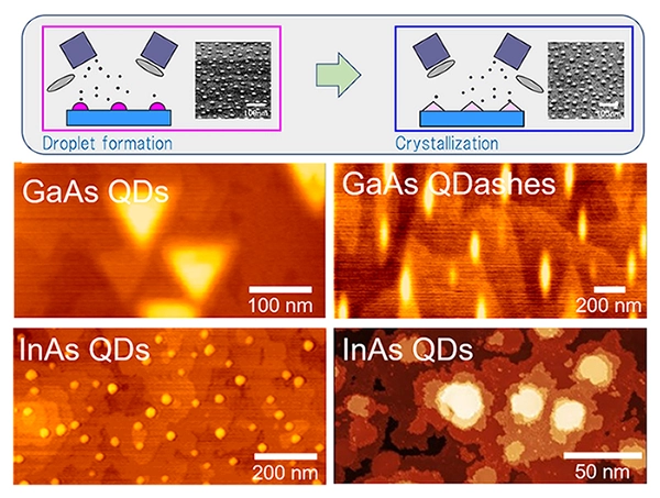
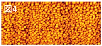
FIG 1 Schematic drawing of droplet epitaxy method and scanning probe microscopy images of GaAs and InAs quantum nanostructures grown by the method.
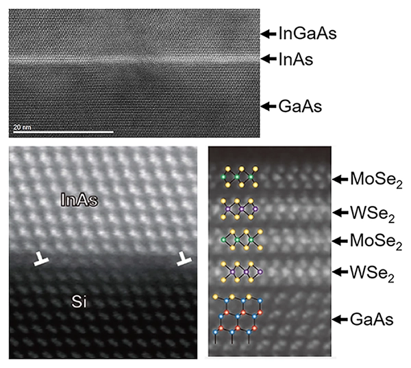
FIG 2 Cross-sectional TEM imaged of various semiconductor heterostructures grown by using advanced epitaxial growth techniques.
MANO, Takaaki / Group Leader
Development of compound semiconductor crystal growth technology and its functional exploration
Overview
III-V compound semiconductor heterostructures are used in various familiar applications, such as light emitting devices, sensing devices, and high-frequency devices. Toward the realization of ioT society in near future, it is necessary to (1) further improve their performance, (2) explore novel functionalities, and (3) realizing price reduction of high quality devices.
Our challenges for solving those issues are developments of novel semiconductor heterostructures by using advanced epitaxial growth techniques and nanophotonics technologies.
Characteristics
Major reserch
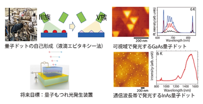
- The self-assembled quantum dots normally exhibit asymmetric shapes due the anisotropy of standard (100) surface. By utilizing our original epitaxial growth method of Droplet Epitaxy, we have succeeded in the formation of highly symmetric quantum dots on (111)A surfaces. We have demonstrated the generation of highly entangled photon pair emission from the QDs.
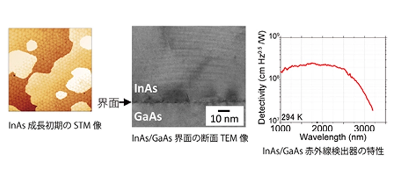
- Narrow bandgap semiconductors-based infrared photodetectors are used in high-quality gas-sensors and night vision cameras. However, they are normally expensive and/or include toxic materials. We have developed highly sensitive InAs-based infrared photodetectors on cheap GaAs substrates by using simple growth method.
Summary
We have developed advanced epitaxial growth technologies of III-V semiconductors and demonstrated novel functionalities of the heterostructures. We will further develop the researches for exploring novel functionalities by integrating various technologies such as theoretical approach, atomic scale analysis, and nanophotonics.
OHTAKE, Akihiro
Development of novel techniques for heteroepitaxy
Overview
We are developing the epitaxial growth techniques for the realization of innovative heterostructures.
By combining advanced growth techniques based on molecular-beam epitaxy and atomic-scale surface/interface characterization techniques, we aim to fabricate atomically-controlled semiconductor heterostructures, mainly focusing on the lattice-mismatched systems.
Characteristics
- Precise control of heteroepitaxy processes based on the atomistic characterization of surface structures.
- Realization of III-V based lattice-mismatched heterostructures by utilizing unique strain relaxation mechanism on (111)-oriented substrates.
- Fabrication of heterostructures consisting of two-dimensional materials such as MoSe2 and WSe2 without constraints of lattice matching.
- In-situ observation of formation processes of quantum dots.
Major reserch
We are studying the growth processes of III-V semiconductors and transition-metal dichalcogenides using a multi-chamber MBE system equipped with STM, electron diffraction, electron spectroscopy apparatuses.
Specific examples are as follows:
- Development of the growth techniques for III-V semiconductors on highly lattice-mismatched substrates such as GaAs(111)A and Si(111), and their application for infrared devices.
- Fabrication of heterostructure consisting of two-dimensional materials such as MoSe2 and WSe2.
- In-situ observation of formation processes of quantum dots grown by droplet epitaxy.
Summary
- We are developing the epitaxial growth techniques mainly for III-V semiconductors and transition-metal dichalcogenides, and investigating their possible application for novel devices.
- Precise control of epitaxial growth processes based on the atomistic characterization of surfaces/interfaces is expected to open the way to realize next generation quantum devices, such as quantum light emitters and advanced sensing devices.
KAWAZU, Takuya
Formation technology of Sb-based compound semiconductor quantum dots
Overview
Stranski-Krastanov (SK) mode growth is one of the widely used methods of quantum dot formation. 10 nm scale quantum dots can be fabricated without dislocations by simply stacking materials with different lattice constants on a substrate. Quantum dots fabricated in this way are expected to be applied to high-performance devices such as semiconductor lasers with excellent temperature stability and high-sensitivity infrared detectors.
In this study, we aim to establish a technology to form, control the shape of, and increase the density of Sb-based quantum dots, which cover a wider range of wavelengths, rather than InAs-based materials that have been widely studied in the past.
Characteristics
- Wide range of density and size control of Sb-based quantum dots by droplet epitaxy
- High density of Sb-based quantum dots on highly indexed surface substrates
- Fabrication of array structures of Sb-based quantum dots by tilted substrates
Major reserch
There is a lattice mismatch of about 7% between GaSb, AlSb and GaAs. When GaSb or AlSb is grown on a GaAs substrate, semiconductor island structures (quantum dots) are formed to relax the strain.
We found that by stacking GaSb or AlSb on high-index GaAs substrates at various substrate temperatures and growth rates, quantum dots with significantly different densities and shapes can be formed.
- GaSb quantum dots on a GaAs(311)A substrate. Density increases by a factor of 1.5 to 2 compared to those on a conventional GaAs(100) substrate.
- GaSb quantum dots fabricated on a GaAs(111)A substrate. Large, flat polygonal dots are formed.
- GaSb quantum dots fabricated on a slightly tilted GaAs(111)B substrate. The dots extend and align along the [-101] direction.
- AlSb quantum dots fabricated on a GaAs(311)A substrate. Small dots are densely formed.
Summary
In this study, we attempted to control the shape of Sb-based quantum dots by selecting parameters such as substrate temperature, growth rate, and substrate orientation. However, optical properties of quantum dots are important for applications in optical devices such as lasers and infrared detectors.
If a method for controlling optical properties can be established based on the knowledge of quantum dot shape control obtained in this study, it is expected to be applied to high-performance optical devices.
IMURA, Masataka
Development of optical, electronic, and magnetic devices using next-generation semiconductors
Overview
In the field of next-generation semiconductor optical, electronic, and magnetic devices, the introduction of wide-gap semiconductors to replace Si is essential. I have focused early on III-nitride semiconductors and diamond semiconductors, which possess excellent applicability, practicality, and high potential, and am developing devices using these materials.
At NIMS, we have established a research system where crystal growth, device processing, and crystal evaluation are integrated, working together with constant feedback.
Characteristics
- Development of radiation and proton detectors using diamond semiconductors
- Development of full-spectrum visible light photonic devices using InGaN-based nitride semiconductor with nanofabrication
- Development of high-efficiency ultraviolet light-emitting diodes using AlGaN-based nitride semiconductors
- Development of high-frequency power devices using AlGaN/GaN and AlInN/GaN heterostructures
- Development of magnetic devices using BAlN and ScAlN-based nitride semiconductors
Major reserch
To realize a highly durable vacuum ultraviolet and proton detector capable of long-term stable operation with low power consumption, we fabricated a vertical Schottky barrier photodiode (SBPD) using diamond and evaluated its basic characteristics and durability.
Conductive diamond substrates were used to reduce charging effects. Low power operation was achieved by operating the device in zero-bias mode.
Furthermore, we evaluated the response characteristics and device durability against vacuum ultraviolet radiation and proton beams.
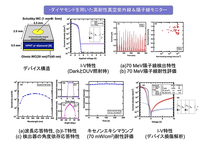
Summary
Using diamond, we fabricated detectors and evaluated their response characteristics and durability when exposed to vacuum ultraviolet radiation and proton beams. The results demonstrated the device's capability for long-term stable operation.
Recently, we have been conducting research and development on full-spectrum visible light photonic devices, high-efficiency ultraviolet light-emitting diodes, high-frequency power devices, and magnetic devices using novel materials, all based on Group III nitride semiconductors.
HAYASHI, Yusuke
Advanced Fabrication and Evaluation Methods for Compound Semiconductor Optical and Electronic Devices
Overview
III-V compound semiconductors have been widely applied to optical and electronic devices such as infrared wavelength laser diodes and high electron mobility transistors (HEMTs) by utilizing their excellent physical properties such as direct transition band gap and heterostructure interfaces.
This research aims to pioneer innovative technologies to drive next-generation semiconductor devices by promoting integration with new material systems and measurements in extreme environments, based on crystal growth technology.
Characteristics
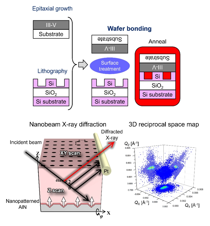
- By utilizing the III-V/Si wafer bonding technology, we aim to achieve fusion with materials that have very large lattice mismatch with III-V semiconductors and to improve the performance of existing material systems, which has not been achieved by crystal growth of existing material systems.
By developing this technology, future silicon photonic optical circuits and optoelectronic integrated circuits using III-V/Si platforms are expected to be realized. - Depth-resolved nanobeam X-ray diffraction measurement using synchrotron radiation can realize strain measurement inside semiconductor devices with high accuracy and high spatial resolution.
By applying nanosecond fast voltage pulses or kilovolt-class high voltage as external signals to semiconductor devices, we can dynamically observe strain behavior and failures under device operation and elucidate physical phenomena under extreme conditions that have not been revealed before.
Major reserch
- The III-V/Si platform can be realized by directly bonding a wafer with eptaxially-grown III-V compound semiconductor light-emitting layers and a silicon-on-insulator (SOI) wafer at a low temperature of 150°C to achieve a defect-suppressed III-V/Si platform. III-V/Si hybrid laser diodes fabricated by this method can be used as a method for integration of light sources on Si-based silicon photonic optical circuits.
- The nanopatterned AlN structure can be measured by nanobeam X-ray diffraction, and the 3D reciprocal lattice map can be measured with depth resolution to determine the strain change induced from the thin film/substrate interface to the sample surface during the AlN crystal growth process.
By developing this method, it can be applied to strain measurement under device operation, and is expected to improve device performance and failure analysis from the viewpoint of strain in the structure embedded inside the device and its vicinity.
Summary
Focusing on optical and electronic devices realized with III-V compound semiconductors, we aim to establish next-generation device fabrication and device operation measurement technologies by integrating new technologies such as wafer bonding and synchrotron radiation measurement, in addition to advanced epitaxial growth technology.
By developing this research, we will work to elucidate physical phenomena under extreme conditions in order to enhance the functionality and reliability of semiconductor devices.
MIYAZAKI, Hideki T. / Managing Researcher
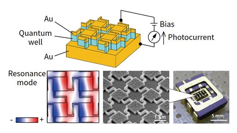
High-sensitivity mid-infrared detectors integrating optical antennas and quantum wells
Overview
Mid-infrared wavelength range (5-10 µm) is important for environmental sensing and security, because molecule-specific absorption and thermal emission appear in this range. However, hazardous mercury and cadmium have been used for conventional high-sensitivity mid-infrared detectors.
In this research, by integrating less hazardous but low-sensitivity quantum-well infrared detectors with unique optical antenna structures, sensitivity comparable to that of conventional detectors has been achieved. The center wavelength can be freely engineered by the design of quantum wells and optical antennas. Therefore, the new detectors are suitable for high-sensitivity detection of a specific gas. Their applications to environmental sensing, agriculture, and medicine are expected.
Characteristics
- Invented a novel optical antenna structure interconnected with zigzag wirings, which enables us high photocurrent extraction while maintaining the synchronized resonance of the whole antennas.
- Integration with optical antennas enhanced the sensitivity of the raw quantum wells by 800 times.
- Resonance wavelength can be freely engineered by the design of the dimensions of the quantum wells and optical antennas.
- Demonstrated comparable or higher sensitivity than conventional detectors, nearly approaching the theoretical limit.
Major reserch
-
Fundamental configuration of an optical antenna is a structure sandwiching a dielectric layer between a top and a bottom metallic layers. By selecting the dimension of each portion properly, the optical antenna resonates at a specific wavelength. In this study, a GaAs/AlGaAs quantum-well photodetector, which exhibits a sensitivity in the mid-infrared range and is less hazardous, is sandwiched between a top and a bottom gold layers. Such optical antennas integrated with quantum wells selectively collect incident light at a specific wavelength, rotate its electric field to a suitable direction for the absorption by quantum wells, and greatly enhance the sensitivity.
Furthermore, by bending the wires interconnecting the antennas into a zigzag shape to adjust the phase f the current, we succeeded in extracting high photocurrent while maintaining the synchronized resonance of the whole antennas. (Arrays of optical antennas are called metamaterials or metasurfaces.)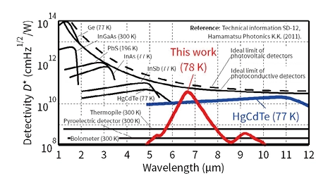
- The absorption wavelength of a quantum-well infrared photodetector can be freely engineered by the thicknesses of GaAs/AlGaAs layers and Al composition. By adjusting the resonance wavelength of the optical antennas with that of the quantum wells and by optimizing the zigzag wires, the sensitivity of the original quantum wells is enhanced by 800 times, and a responsivity of 3.3 A/W (at 6.7 µm and 78 K), an external quantum efficiency of 61%, and a detectivity of 3.9×10¹⁰cmHz1/2/W were achieved. This detectivity is higher than those of HgCdTe photodetectors, conventionally used as high-sensitivity detectors, and nearly approaching the theoretical limit. The responsivity has a sharp peak at a specific wavelength, thus, our detector is suitable for measuring the concentration of a specific gas. We also demonstrated fast measurement of NO2 gas concentration (absorption wavelength 6.25 µm) at a response time less than 1 ms.
Summary
By integrating optical antennas and quantum wells, we demonstrated high-sensitivity mid-infrared photodetectors with comparable performances of conventional detectors without using hazardous materials. Because the center wavelength can be freely selected by the design of the quantum wells and optical antennas, our detector is suitable for sensors detecting a specific gas with a high sensitivity.
By raising the operation temperature based on the structure optimization and by further integration of the devices, we would like to apply our detectors to environmental sensing, agriculture, and medicine.
Current Members (as of 2026)
Specially Appointed Research Fellow
SAKUMA, Yoshiki SAKUMA.Yoshiki@nims.go.jp

