 IWANAGA.Masanobu@nims.go.jp
A photo of a metasurface substrate (with 6 channels) is shown in (A). White scale bar indicates 10 mm. The magnified image shows an electron microscopy image. This metasurface comprises periodic array of Si nanocolumns with 300 nm periodicity. The height of the nanocolumn is 200 nm. Black scale bar indicates 500 nm. This metasurface was designed to have highly FL-enhancing feature at wavelengths of 570-600 nm.
[M. Iwanaga, Biosensors 13, 377 (2023).]
Nanophotonics Group | Research Center for Electronic and Optical Materials

Nanophotonics Group
Group leader
Group members
AIM and GOAL
Our research targets are nanophotonics materials such as metasurfaces (metamaterials) and photonic crystals, composed of subwavelength-sized structures. We will create artificial materials with peculiar optical functions never attained in nature by precise design and high-accuracy fabrication.
In addition to the applications of nanophotonics materials to sensors, etc., we will also focus on fundamental researches for exploring novel physics.
APPROACH
Our highly engineered nanophotonics materials are produced by both approaches: the top-down nanofabrication and the bottom-up self-assembly. We are developing metasurfaces with precise surface structures suf ficiently smaller than the optical wavelength and applying them to biosensors and infrared detectors.
We are developing three-dimensional self-assembling techniques of spherical colloidal particles and colloidal quantum dots, and e xtending their application to strain imaging and lasers.

FIG 1 Metasurface biosensor to detect a target DNA at ultrahigh sensitivity (top). Metasurface infrared dual-wavelength detector for measuring the concentration of a specific gas (bottom).

FIG 2 Roll-to-Roll continuous growth of colloidal photonic crystals (left). High-quality thin film made of perovskite quantum dots (right).
IWANAGA, Masanobu / Group Leader
Optical Metasurface Biosensor System
Overview
Going through the global pandemic caused by the COVID-19, it is widely recognized that biosensing technologies are crucial in society. In particular, sensing technologies that can detect diverse target biomolecules in a very high-sensitivity, specific, and short-time manner are highly demanded. However, pursuing extremely high sensitivity resulted in current large and cost-demanding inspection instruments, which are mismatched with actual demands. Considering these situations, we have developed a new type of biosensing technology.
Metasurfaces are nanostructured surfaces that exhibit particular functions owing to the artificial designs based on precise simulations, and are extensively studied in a global scale. We experimentally found metasurfaces extremely enhancing fluorescence (FL) among the diverse metasurfaces and applied the FL-enhancing metasurfaces to FL biosensing. To date, we have succeeded in highly precise detection of various target biomolecules across proteins such as cancer-marker antigens and nucleic acids such as cell-free DNA.
Characteristics
- We found highly FL-enhancing metasurfaces on our own in NIMS.
- This FL-enhancing metasurfaces are ranked at the top in the world.
- Employing the metasurface biosensors, cancer marker antigens are detected, even when they are in tens fold lower concentrations than the medical diagnosis criterions.
- Combining with short-cycle nucleic-acid amplification techniques, we achieved ultimate single-molecule sensing that can discriminate one DNA from zero.
- This ultimate sensing of single-molecule DNA molecule has never been realized using any other technique such as digital PCR method.
Major reserch

A scheme to detect cell-free DNA is shown in (B). A specific cell-free DNA sequence that is induced in practice effect was set to be the target. We went through 30-cycle nucleic acid amplification (usually, more than 40 cycles are conducted and more than 1000-fold amplification is done; however, falsely positive reactions happen with higher probabilities). The amplified products were labeled with biotin and FL probes, which enables us to efficiently immobilize target amplicons on the metasurfaces. At the right-hand side, the FL emission is schematically illustrated. Through this detection protocol, we demonstrated ultimate single cell-free DNA detection that can discriminate one molecule from zero.
[M. Iwanaga et al., Nano Letters 23, 5755 (2023).]
Overall, we established a simple setup with extremely high sensitivity. This biosensor system makes the detection of next-generation biomarkers such as microRNA feasible. We aim at contributing to creation of new healthcare services.
Summary
- We have developed metasurface FL biosensors with extremely high sensitivity and the automated detection system.
- This system is applicable for various situations across protein and nucleic acid detections.
- We have attained ultimate sensing performance of single-molecule detection regarding extremely low-concentration DNA.
FUDOUZI, Hiroshi
High-quality colloidal crystal thin film coatings and smart structural color functional materials
Overview
Colloidal crystals, comprising colloidal particles of uniform size arranged in a 3D regular order, are classified into two types: the closest-packed type and the non-closest-packed type. NIMS has been conducting pioneering research on process technology and structural color materials for both types of colloidal crystals. For instance, photonic rubber is a novel elastic material that undergoes a reversible structural color change through deformation.
Concurrently, we have developed a strain visualization sheet that enables the observation of cracks and deformation in infrastructure through color changes. This technology is anticipated to facilitate the visual inspection of abnormalities in aging infrastructure, which are increasing at a rapid rate, or using a smartphone. Furthermore, we have established a coating process technology for forming a homogeneous, uniform, highly crystalline colloidal crystal film with a surface area of 1000 cm2.
Characteristics
- Colloidal photonic crystal film deposition process (with face-centered cubic lattice (111) plane orientation, number of layers controlled)
- Large-scale production up to A3 size and coating on curved surfaces (lab-level production)
- Smart film material that visualizes stress and strain using structural color (visualization of structural color changes due to deformation)
- Practical application needs: strain visualization sheet (weather resistance), photonic rubber (durability)
- Production of colloidal particle suspensions (particle concentration: 10 wt% - 20ℓ, particle diameter from 150 to 450nm)
Major reserch 1
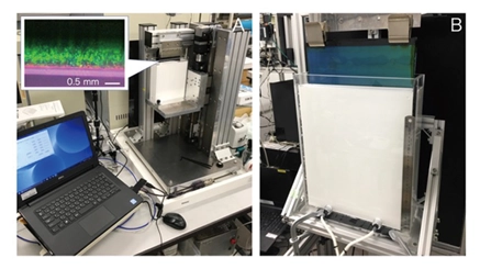
[Colloidal crystal thin-film coating by oil-covering method]
A: A vertical deposition device for high-quality colloidal crystal thin films. The inset photo shows an enlarged image of the interface area. Non-close-packed colloidal crystals are formed through an Alder phase transition that occurs as the colloidal suspension evaporates and becomes more concentrated. The structural color changes from red to green (the particle interspacing decreases), and finally a close-packed colloidal crystal thin film is formed. The substrate is fixed, and the suspension tank mounted on the stage moves downward to form a colloidal crystal film on the substrate surface.
There are two types of stage drive control: one that sets a constant speed and another that uses a reflective optical fiber to measure crystallization and feeds the results back to the stage drive motor.
B: A film deposition system that has been scaled up to A3 scale size. In addition, a coating system that uses a pump suction method without stage drive has also been developed.
Major reserch 2
[Structural color materials using colloidal crystal thin films]
A: Coaxial irradiation photography, a colloidal crystal thin film composed of polystyrene colloidal particles and silicone elastomer on a polyvinylcarbonate, PVC thermoplastic sheet. The structural color can be selected from red to blue by heating and deforming the sheet, and the structural color also changes with the shift in wavelength position of the Bragg diffraction peak in the visible light region.
B: Photonic rubber with the structural color changes reversibly with elastic deformation. Durability tests were conducted on repeated deformation, and it was confirmed that it still functions as photonic rubber even after 250,000 repetitions of stretching.
C: Strain visualization sheet, the cracks that occur in the bending test during on-site construction of a concrete bridge turn green, and a surface protective layer is formed on the strain visualization sheet that is exposed outdoors and used (weather resistance of about 5 years was confirmed by the exposure test in outfield).

Summary
We provide test specimens, such as high-quality colloidal crystal thin films, photonic rubbers, and strain visualization sheets in A3 size. We can also provide technical transfer of the film deposition process. In addition to structural colors, we can also use photonic band gaps to make optical filters that include the near-infrared region.
We are currently developing a roll-to-roll continuous film deposition process that will allow us to produce these products on a large scale.
HO, Ya-Lun
Overview
Low-dimensional materials have emerged as promising candidates for applications in nanophotonics and optoelectronics due to their unique optical properties and atomic scale. A major issue in developing practical low-dimensional materials-based nanophotonic devices is realizing photonic structures via on-chip fabrication with low-dimensional materials, enabling strong light-matter interaction within atomic scale.
In my research, I design and develop nanophotonic, plasmonic, and metasurface platforms, as well as original nanofabrication techniques, specifically tailored for low-dimensional materials.
Characteristics
- High-quality low-dimensional material-based nanophotonic structures for on-chip integrated devices
- Large-area and non-transfer top-down nanofabrication technologies tailored to colloidal quantum dots and 2D materials
- Compatibility with well-established semiconductor fabrication processes
- Nanophotonics and metasurface design enabling efficient coupling of light into the atomic scale, ensuring strong light-matter interaction and high quality factor
Major reserch
Here, the works based on perovskite QDs, including on-chip integrated single-mode lasers, nanolaser-waveguide coupled photonic circuits, metasurface-based surface-emitting lasers, and plasmonic hot-electron photodetection devices, have been developed and presented by utilizing superior quantum efficiency and recrystallization properties of perovskite QDs.

Summary
My research positioning is to bring the potentials of low-dimensional materials into real integrated nanophotonics by coupling these advanced photonic materials, new-design nanophotonic platforms, and original on-chip nanofabrication, and further to push the limits of nanophotonics via low-dimensional materials.
Current Members (as of 2026)
Postdoctoral Research Fellow
SAHOO MihirKumar SAHOO.MihirKumar@nims.go.jp
Project Technical Staff
TSUDA, Chikako TSUDA.Chikako@nims.go.jp
TERUI, Kaori TERUI.Kaori@nims.go.jp
Temporary Staff(engineering)
HIRONAKA Takashi HIRONAKA.Takashi@nims.go.jp
Visiting Researcher
DENG Chih-Zong DENG.Chih-Zong@nims.go.jp
DEGA Naresh Kumar DEGA.NareshKumar@nims.go.jp

