 OHASHI.Naoki@nims.go.jp
Metal oxide semiconductors such as ZnO and SnO2 have long been studied for gas sensing applications, such as medical expiratory gas sensor and air pollution monitoring, as they can easily achieve high sensitivity and miniaturization and are inexpensive due to their simple structure. However, for these applications, there is a demand for sensors with even higher sensitivity and improved gas selectivity.
The film thickness of a thin-film type gas sensor is a parameter that greatly affects the sensor response value, and it is expected that the thinner the film, the better the sensor response value. Until now, most reports have been on sensors with a film thickness of several tens of nm or more. We have demonstrated that the sensor response improves dramatically by reducing the film thickness of a metal oxide semiconductor to about 10 nm.
In addition, which crystal face is exposed on the surface of metal oxide semiconductor crystals greatly affects the gas selectivity of the sensors. Polar crystals such as ZnO have crystal faces terminated by Zn or O atoms, so it is expected that the gas selectivity will differ depending on which crystal face is on the top surface. We have developed a process to control the crystal plane exposed on the top surface of ZnO thin films and have demonstrated that sensors with different gas selectivity can be fabricated using the same material.
These results will be useful for designing gas sensors with high sensitivity and high gas selectivity.
Electro-ceramics Group | Research Center for Electronic and Optical Materials

Electro-ceramics Group
Group leader
Group members
AIM and GOAL
Elecroceramics are ceramics exhibiting functionality, including dielectric, conductive, magnetic, and optical properties, originated in behavior of electrons, and are utilized in electronic devices, such as computers, and electric facilities, such as power stations. Those are not only in chip form but also in various forms, e.g., films on wafers etc.
This group is engaged to obtain further higher functionality of electroceramics and technology for production of new electroceramics aiming to contribute development of information technology and energy saving systems.
APPROACH
This group performs exploration of new compounds and materials based on theoretical prediction and accumulated knowledge, and characterization of electronic structure of those materials. In particular, this group aims to realize new semiconductors, piezoelectric/ferroelectric materials exhibiting non-traditional functionality. In addition, this group pays attention to functionality originated at surface and interfaces: hence, this group also concentrates on development of new processes, such as growth of epitaxial film and construction of nanostructures composed of crystalline and non-crystalline materials.
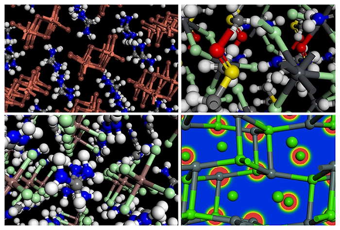
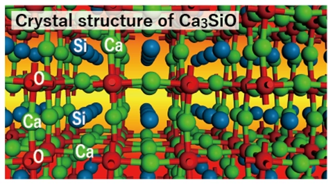
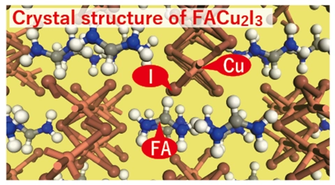
FIG1 Exploration of new crystal structures, e.g., organic-inorganic hybrid crystals. and search on new functionality utilizing ab-initio calculations.
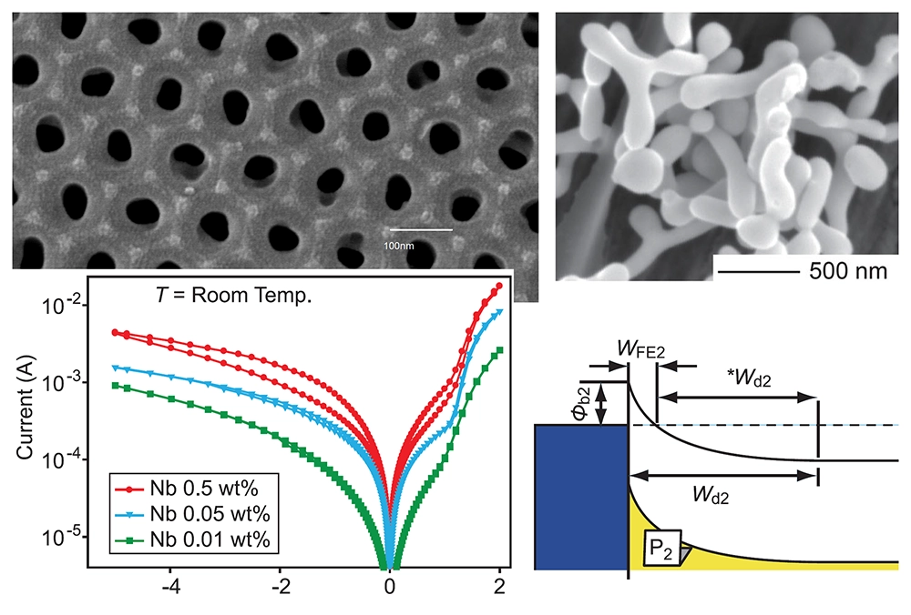
FIG 2 Development of new processes for fabrication of nano-structures and exploration of new functions at surfaces and interfaces
ADACHI, Yutaka
Improvement of gas sensing properties of metal oxide semiconductor thin films
Overview
Metal oxide semiconductors are used as gas sensors because their electrical resistance changes in response to the gas concentration in the air, and there is currently a demand for the development of sensors with higher sensitivity and gas selectivity. In the case of thin film form, it is expected that the sensing response will improve as the film thickness is reduced, but most reports have been on sensors with a film thickness of several tens of nm or more. We have demonstrated that the sensor response improves dramatically by reducing the film thickness of a metal oxide semiconductor to about 10 nm.
In addition, we have revealed that the crystal plane exposed on the surface of the metal oxide semiconductor gas sensor has a significant effect on the gas selectivity. We have developed a process to control the crystal plane exposed on the surface of ZnO thin films, and have demonstrated that sensors with different gas selectivity can be fabricated using the same material.
Characteristics
- We have demonstrated that the sensor response improves dramatically by reducing the film thickness of a metal oxide semiconductor to about 10 nm.
- We have developed a process to control the crystal plane exposed on the surface of ZnO thin film.
- We have revealed that the crystal plane exposed on the surface of the metal oxide semiconductor gas sensors has a significant effect on the gas selectivity.
Major reserch

Summary
The results of this research will contribute to the development of gas sensors with high sensitivity and selectivity, which are expected to be applied to portable breath analysis devices and environmental gas monitoring systems.
OHSAWA, Takeo
Creating functional properties in oxide interface structures
Overview
Integrating oxide materials with diverse functionalities at the atomic level to create unprecedented new properties is becoming increasingly important for realizing an energy-efficient and energy-generating society. In pursuit of highly efficient oxide-based devices, perovskite-type oxides (mainly SrTiO3and BaTiO3) and polar oxide semiconductors such as ZnO heterostructures have attracted significant attention.
By utilizing advanced thin-film growth techniques with atomic-level precision, I aim to develop ultra-high-quality semiconductor devices with reduced impurity and defect densities, with the goal of enhancing device performance and advance material development for next-generation technologies.
Characteristics
- Atomic-level control of structure, composition, and defects for the formation of high-quality junction interfaces
- Measurement techniques for ultra-trace impurities and their application in unveiling hidden functionalities
- Establishing property correlations by integrating imaging, spectroscopy measurements, and electronic transport data
Major reserch
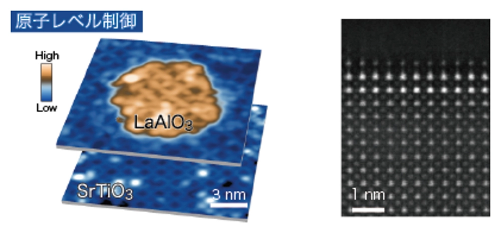
- By fabricating an epitaxial structure with atomic-level precision at the oxide heterointerface, the spatial distribution of electronic states was measured with atomic-level resolution, elucidating a unique growth mode. Additionally, this interface successfully accumulated a high concentration of electrons, leading to the emergence of novel electronic properties.
- A method for controlling the polarity of wurtzite-type ZnO thin films was established, revealing associated modulations in electronic properties. Furthermore, the study clarified electron transport mechanisms originating from reduced impurities and defect structures in high-quality ZnO crystals, providing insights that can be developed for new process applications.
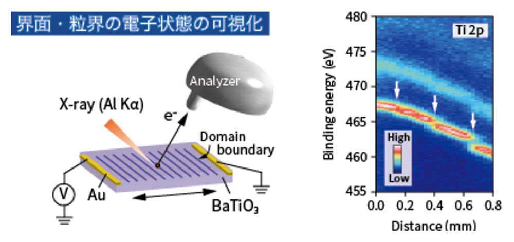
- Anisotropic electrical conductivity and local electronic states based on ferroelectric domain structures in BaTiO single crystals were successfully observed. By employing photoelectron spectroscopy, the potential barriers at domain boundaries were visualized.
- To investigate the operation mechanism of resistive switching memory, the interfacial electronic states were elucidated using bulk-sensitive hard X-ray photoelectron spectroscopy. This research led to the development of a process for creating high-speed memory based on the newly discovered mechanisms.
1
2

3

4
Summary
- Measurement of electronic states at oxide thin film interfaces and domain boundaries
- Determination of the polarity of polar oxide semiconductors using electron spectroscopy
- Elucidation of electron transport properties via polarity control
- Creation of diverse properties through high-quality heterojunction formation
- Development of new principles for the creation of practical devices
- Establishment of precise defect control technologies in oxides
SAITO, Noriko
Semiconductor metal oxides gas sensors
Overview
Recently, expectations for gas sensors have increased, not only for conventional alarms that contribute to safety and security but also in the fields of health and the environment, as well as for more comfortable living and the creation of a sustainable society. Furthermore, there is a demand for miniaturization, energy savings, and implementation in mobile and wearable devices. Metal oxide semiconductors function as gas sensors because their electrical resistance changes depending on the amount of oxygen ions adsorbed on the surface. The surface is important for improving the sensor sensitivity.
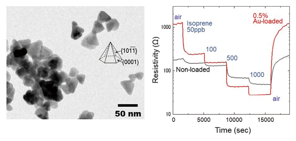
We synthesized ZnO particles with a novel shape and investigated the effect of their crystalline surface on the sensor and gas desorption properties. In addition, practical application issues were examined.
Characteristics
- Shape and crystal facet control of metal oxide ceramic powders
- Evaluation of gas sensor properties of pyramid-shaped zinc oxide particles loaded with Au nanoparticles
- Detection of isoprene gas at 10 ppb to 1 ppm under high humidity
- Available for breath analysis
Major reserch
To determine the physical conditions, a wellness sensor capable of detecting small amounts of gases in exhaled breath are expected. Isoprene is a gas exhaled when people are sleepy, and this gas sensor is believed to be useful in preventing overwork and automobile accidents.
We studied the microstructure control of zinc oxide particles (left figure) and catalyst addition; isoprene gas equivalent to the concentration in exhaled breath was detected under high humidity conditions (right figure).
Exposure of the active crystal surface, which has many oxygen defects that serve as oxygen ion adsorption sites, was effective in improving sensitivity. This sensor showed the highest sensitivity among metal oxide semiconductor isoprene sensors.
Summary
We developed zinc oxide gas sensors that can detect ppb-level gases by controlling crystal facets and nanostructures. Highly sensitive gas receptor particles can be used in wellness sensors, air quality monitoring sensors, and breath gas health diagnoses.
Future practical applications will require improved gas selectivity and miniaturization for installation in mobile devices.
UEDA, Shigenori
Interface electronic states studied by utilizing X-ray total reflection
Overview
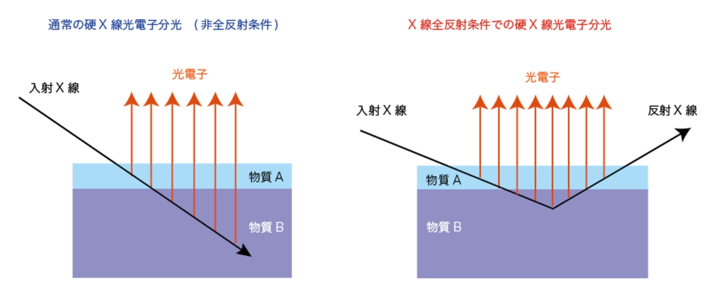
Hard X-ray photoemission spectroscopy (HAXPES) can probe bulk-sensitive electronic structures of solids due to a larger probing depth compared to conventional PES.
The large probing depth in HAXPES is a strong advantage to probe electronic and magnetic states of buried interfaces of functional devices in non-destructive way, which will provide a guiding principle for improving device properties. To investigate electronic and magnetic states near interfaces of device structures, we have developed a powerful method: a combination of HAXPES with X-ray total reflection.
HAXPES combined with X-ray total reflection enables us to observe band offsets in semiconductor heterostructures and electronic and magnetic states near interfaces of insulator/ferromagnet structures.
Characteristics
- Tuning of escape depth of photoelectrons by utilizing X-ray total reflection
- Non-destructive observation of near-interface electronic states
- High-speed (10 times faster) depth-dependent measurements compared to conventional method
- Detection of band offset and band bending properties in semiconductors
- Detection of magnetic information on ferromagnets combined with circularly polarized X-rays
Major reserch
When HAXPES measurements are performed in non-X-ray total reflection conditions, a photoelectron intensity from a deep region becomes larger than that from a surface region. In contrast, in the case of the X-ray total reflection condition, a photoelectron intensity from the interface between material A and B is enhanced (if material A is absent, a photoelectron intensity from the surface of material B is enhanced).
HAXPES with a tuned X-ray attenuation length by utilizing an X-ray total reflection at around its critical angle, we have successfully detected a surface band bending of widegap semiconductors. In addition, the application of HAXPES combined with X-ray total reflection revealed that the magnetization near interface reduces compared to the bulk region for insulator/ferromagnet structures.
Since this method can probe band offsets in semiconductor heterostructures and electronic and magnetic states around interfaces of insulator/ferromagnet structures, it is expected that the observed results provide essential knowledge for improving device properties.
Summary
We have realized high-throughput depth-dependent electronic structure measurements by using HAXPES combined with X-ray total reflection.
The direct observation of surface band bending of semiconductors, band offset in semiconductor heterojunctions, and electronic and magnetic states near interfaces of insulator/ferromagnet structures will provide essential knowledge for improving device properties.
SHIMIZU, Takao
Exploration of novel non-perovskite ferroelectric and Pb-free piezoelectric materials
Overview
Ferroelectric materials can exhibit the attractive characteristics, such as piezoelectricity, pyroelectricity, and ferroelectricity, because of their crystal structure. They have been expected to be applied to various devices including sensor, actuator, and non-volatile memories. However, the conventional ferroelectric materials cannot meet recent requests for the miniaturization and elimination of the toxic element. Hence, novel ferroelectric materials are highly demanded.
We investigate and develop new ferroelectric materials, Pb-free perovskite materials, HfO2-based and wurtzite type ferroelectrics, which is out of the conventional composition and crystal structure.
Characteristics
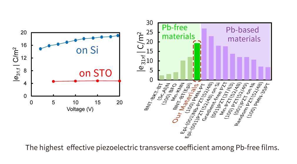
- Development new Pb-free piezoelectric materials with excellent electro-mechanical properties (d33≈275 pm/V and e31, eff ≈ 19 C/m2)
- Demonstration of the ferroelectricity of HfO2 film over 1μm thick, which had been considered to show ferroelectricity in ultra-thin film less than 100 nm thick.
- Expansion of composition and thickness range of wurtzite-type ferroelectrics.
Major reserch 1
Lead zirconate titanate(PZT), which has been utilized as piezoelectric material for many decades, show high electro-mechanical coupling at the boundary between tetragonal and rhombohedral phases. To obtain large electro-mechanical coupling in Pb-free materials, the searching the phase boundaries has been conducted conventionally. By contrast, we have achieved the highest piezoelectric performance in tetragonal 0.7(Bi0.5Na0.5)TiO3-0.3BaTiO3 among Pb-free piezoelectric films, by harnessing domain rotation (partial rotation of crystal lattice).
Because this concept is insensitive to fluctuation of the composition, it can be applied to various ferroelectric materials. The high-performance piezoelectric material in this study enables miniaturization and increase in output of electro-mechanical-micro-systems.
Major reserch 2
Recently, ferroelectricity has been reported in HfO2-based films, which have excellent CMOS compatibility, and in wurtzite-based polar materials, of which polarization can never be switched. In the study of the mechanism for the appearance of ferroelectricity, we demonstrated ferroelectricity in HfO2-based films over 1μm thick, although they only show ferroelectricity in ultrathin films less than 100 nm thick. This finding allows HfO2-based films to be used in other applications, such as piezoelectric sensors and actuators, in addition to non-volatile memory. Furthermore, we also address the extension of the composition and thickness ranges showing ferroelectricity in wurtzite-based ferroelectric materials, whose giant polarization is of great advantage for ferroelectric non-volatile memories.

Summary
- Exploring new piezoelectric materials using polarization (domain) rotation.
- Piezoelectric and pyroelectric application of HfO2-based film.
- Device application in polarization inversion of wurtzite-based materials.
SUEHIRO, Takayuki
Powder Synthesis of Functional Nitrides
Overview
Recently, SiAlONs and nitridosilicates have been developed as an important class of phosphors for solid-state lighting (SSL), whereas their low manufacturability is a major obstacle to the widespread use in SSL applications, triggering intense investigations for developing a sophisticated powder synthesis technique for nitride materials.
We developed the Gas-Reduction—Nitridation (GRN) method, which enables direct synthesis of nitride fine powders from inexpensive and stable oxide raw materials utilizing an ammonia-hydrocarbon gas mixture as a reduction—nitridation agent, focusing on their applications to SSL and novel photocatalytic energy production.
Characteristics
- The GRN method enables direct synthesis of nitride fine powders from inexpensive and stable oxide raw materials utilizing ammonia-hydrocarbon as a reduction—nitridation agent
- Morphologically characteristic nitride fine particles can be synthesized by the GRN process
- Various alkaline-earth/rare-earth nitridosilicate phosphors can be produced by the GRN process without using air-sensitive nitride raw materials
- Quaternary or higher multinary nitrides can be precisely synthesized by the GRN method
- Solar-active photocatalysts have been developed by synthesizing novel multinary nitrido-germanates/gallates
Major reserch
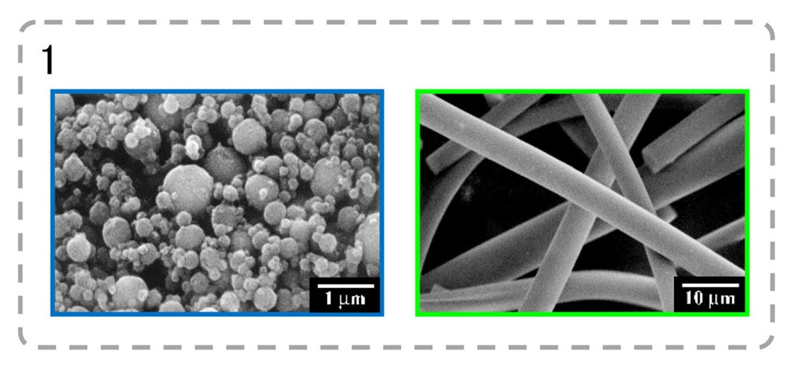
- Morphologically tailored high thermal conductive AlN fillers, such as spheres, micro fibers, and nanoparticles have been synthesized by utilizing the GRN process.
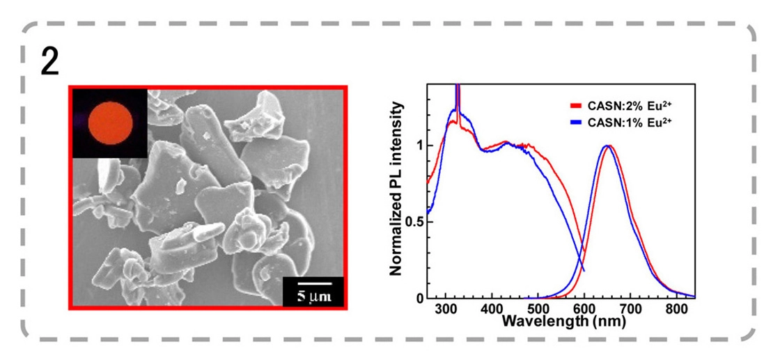
- The GRN synthesis of platelet CaAlSiN3:Eu2+ fine powder phosphors has been achieved, enabling precise tuning of PL properties with high EQE of 72%.
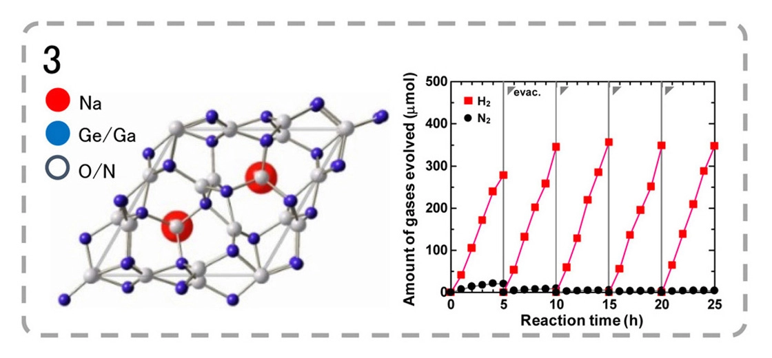
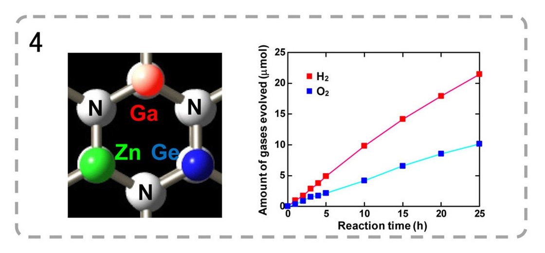
- A novel SiAlON analogue, Na-α-GeGaON has been synthesized by the GRN, demonstrating stable photocatalytic hydrogen generation from water under UV irradiation.
- A novel quaternary wurtzitic nitide photocatalyst, Zn1-xGe1-xGa2xN2 has been developed, demonstrating overall water splitting under visible-light irradiation of λ > 400 nm.
Summary
- The GRN process has been successfully applied to the synthesis of morphologically characteristic, high thermal conductive nitride filler particles
- The GRN process can be adopted for industrial production of various nitride fine powder phosphors for SSL
- Development of novel multinary nitrides will enable photocatalytic solar-hydrogen production in the future
SUMIYA, Masatomo
Development of novel functions from the formation of heterostructure composed of polar nitride semiconductors
Overview
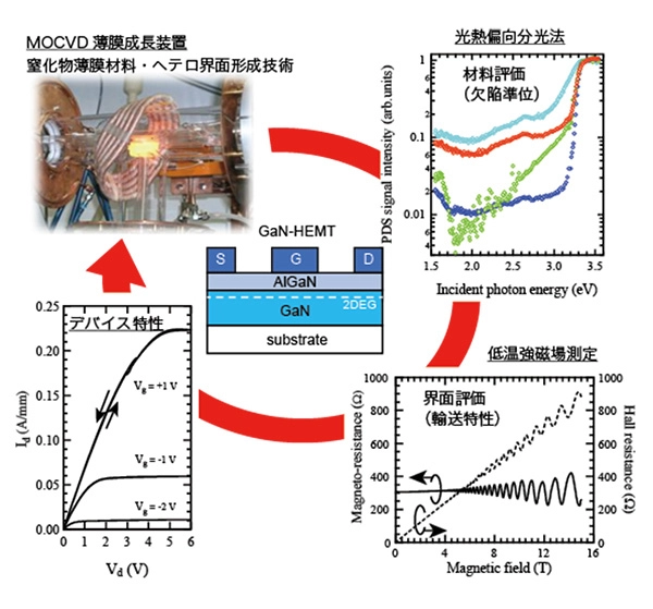
I have studied the mechanism of polar direction of nitride semiconductor film by metalorganic chemical vapor deposition. Unique electronic state is formed at the heterointerface of AlGaN/GaN by the polarity along c-axis (spontaneous polarization) and in-plane strain (piezo electric field). The defect levels in the bandgap are characterized by photothermal deflection spectroscopy The carrier transport of two-dimensional electron gas at the heterointerface is investigated under the high magnetic field at low temperature. Improving the nitride semiconductors and understanding the physical properties, novel functions will be developed from the formation of heterostructure composed of polar nitride semiconductors.
The achievements will be resulted in the high electron mobility transistors and photoelectric conversion devices.
Characteristics
Growing nitride semiconductor samples by metalorganic chemical vapor deposition, I have studied the basic physical properties such as defects in the bandgap, carrier transport at 2DEG, and surface oxidation for improving the device performance of LED, HEMT, and photovoltaic. The system of photothermal deflection spectroscopy has been developed originally for nitride semiconductor materials to detect the defect levels in the bandgap. 2DEG carrier transport has been analyzed together with a collaboration with the magnetic field group in NIMS. Theoretical GaN surface model taking the polarity into account was realized through the collaboration with RIKEN researcher.
Major reserch
I prepare the nitride semiconductor samples on the various substrates such as AlN templates /sapphire or SiC and GaN bulk substates by MOCVD. 2DEG carriers induced at the interface AlGaN/GaN and AlGaN/InGaN heterostructures exhibit Shubnikov de Haas (SdH) oscillation. The HEMT devices processed from these samples exhibited the good performance. Photothermal deflection spectroscopy (PDS) can detect the defect density as low as ~1014 cm-3 of order or less. The mechanism of in-gap emissions was discussed in the viewpoint of structural disorder or defect in the bandgap evaluated by PDS. Oxidation behaviors on various GaN surfaces were provided with the experimental data and molecular dynamics calculation.
Summary
- Nitride semiconductor materials of film and heterostructures grown by MOCVD
- Evaluation of defect levels in nitride semiconductors by PDS
- Characterization of 2DEG transport in high magnetic field at low temperature
- Theoretical and experimental approach to the surface oxidation on nitride semiconductor surface
- Improvement of performance composed of nitride semiconductors.
Current Members (as of 2026)
Postdoctoral Research Fellow
OKAMOTO, Atsuro OKAMOTO.Atsuro@nims.go.jp
Graduate Research Assistant
YOSHIDA, Seiyo YOSHIDA.Seiyo@nims.go.jp
Project Technical Staff
TASAKI, Midori TASAKI.Midori@nims.go.jp
SESOKO, Miho SESOKO.Miho@nims.go.jp
Temporary Staff(engineering)
NAKAJIMA, Miho NAKAJIMA.Miho@nims.go.jp
SAWABE, Yoshinari SAWABE.Yoshinari@nims.go.jp
DENPOYA, Keiko DENPOYA.Keiko@nims.go.jp
Visiting Researcher
BEN MILED Marwan BENMILED.Marwan@nims.go.jp

