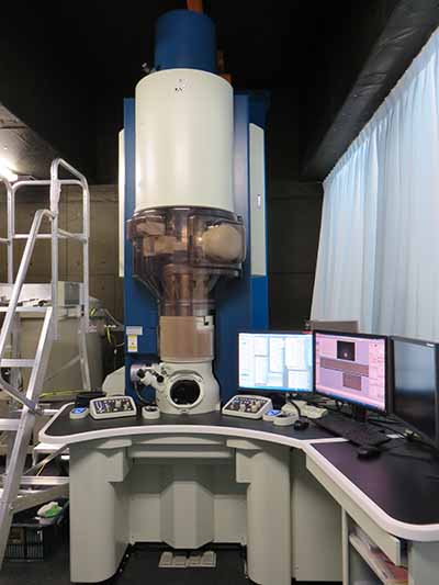
施設・装置Facilities
実動環境対応型電子線ホログラフィー電子顕微鏡 (JEM-ARM200F-B) Real Working Environmental Electron Holography Microscope
[設置部屋] 千現地区 ファインプロセス実験棟125室/Location: Room125, Fine Processing Laboratories Building
[メーカー] 日本電子/Maker: JEOL Ltd.
照射レンズ系、結像レンズ系のそれぞれにCEOS社製収差補正器CESCOR,CETCORを搭載し、空間分解能は0.08 nmに達します。冷陰極電子銃により低加速電圧でも高分解能STEM が可能です。バイプリズムも装着しており、ポテンシャル計測も可能です。OriusSC200(Gatan社),965 GIF Quantum ER(Gatan社)を装着しておりEELS,エネルギーフィルタ像の取得が可能です。
This microscope has TEM image and STEM probe aberration correctors for high-resolution observations. Cold FEG enables high-resolution STEM even at low acceleration voltage. EELS and energy filter image acquisition is possible.
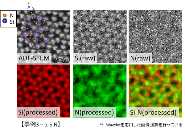
試料としてαタイプSiNを用いた。処理を施したNマップを見ると、強度は確かにNサイトで高くなっていることがわかる。一般にEDSは軽元素には不向きといわれているが、結晶性試料のようにチャネリングが利用できる場合原子分解能においても全く不可能でないことが分かる。
The specimen used is an a-type SiN. You can see from the processed N map, that the strength is certainly stronger on the N site.
Typically, it is said that EDS is not suited for light elements, but if channeling can be used as in the case of crystalline samples,
EDS analysis is not impossible even for atomic resolutions.
| Specifications | |
|---|---|
| Acc. Voltage | 200 kV, 80 kV, 60 kV with a Cold FEG and 2 Cs correctors (CL and OL) |
| Resolution | Point 0.11 nm / Lattice0.07 nm (TEM mode) 0.08nm (STEM mode) |
| Sample Tilting Angle | X / Y=±35° / ±30° |
| Observation/analysis functions |
・EELS analysis: GATAN Quantum (200 kV, 80 kV, 60 kV) ・EDS: Dual SDD Type (Detection surface area 2 × 100 mm2; Solid angle 1.96 sr=2 × 0.98 sr) ・Electron holography: Wave-front separation holography by use of an electron biprism |
| Environmental functions | ・準備中 |