TSUCHIYA Takashi
Group Leader, Neuromorphic Devices Group, Research Center for Materials Nanoarchitectonics (MANA), National Institute for Materials Science
 NIMS
researchers directory, SAMURAI
NIMS
researchers directory, SAMURAI
 How to
 Send email
Research field
neuromorphic computing, brain-inspired computing, ionics, iontronics
Research outline
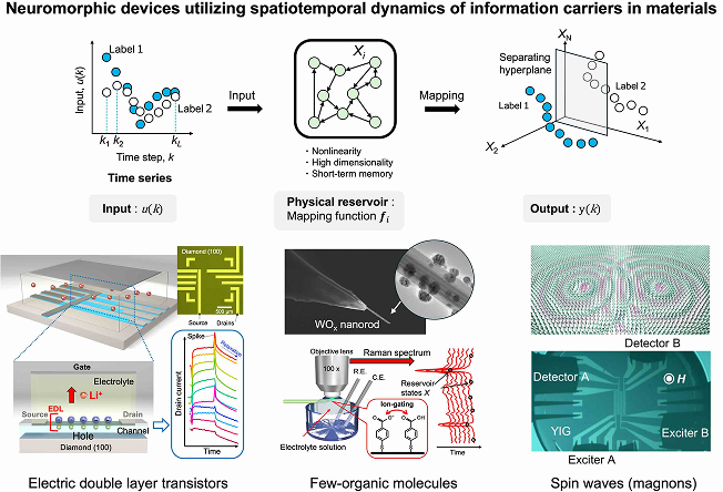
In recent years, the problems of high power consumption, high data traffic, and high latency in machine learning have become more serious. To solve this, we are developing neuromorphic devices that perform information processing as efficiently as the human brain by utilizing the spatiotemporal dynamics of information carriers such as ions, electrons, and spins in materials.
Research Interests
neuromorphic devices, reservoir computing, edge AI, resistive random access memory, ion-conducting materials
Assigned university/courses
Waseda University Graduate School of Advanced Science and Engineering
Department of Nanoscience and Nanoengineering
Message to prospective students
In our laboratory, researchers and students from a variety of fields bring their ideas together, discuss them freely, and support each other as they carry out their research. Let us seek for ground breaking neuromorphic devices enabling extremely-low power consumption AI and enriching human life.
OHKUBO Isao
Principal Researcher, Thermal Energy Materials Group, Nanomaterials Field, Research Center for Materials Nanoarchitectonics (MANA), National Institute for Materials
Research field
Nanoscale-controlled thin-film growth, Electronic structure calculation, Thermoelectric & electronic devices, Informatics
Research outline
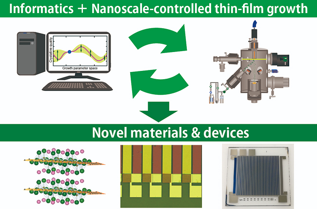
Development of novel functional materials and devices (thermoelectric and electron transport properties) by utilizing the various informatics approaches (first-principles calculations, databases, machine-learning approaches etc.) and nanoscale-controlled thin-film growth techniques is carried out.
Research Interests
Molecular beam epitaxy, Microfabrication, First-principles calculations, machine-learning, database approaches
Assigned university/courses
University of Tsukuba Graduate School of Pure and Applied Sciences
PhD : Materials Innovation
MSc : Materials Innovation
Message to prospective students
Students from various fields (chemistry, physics, materials science etc.) are welcome to participate. Research works can be implemented based on own area of expertise. Let's enjoy research works to the fullest!
FUKATA Naoki
Field Director, Quantum Materials Field, Research Center for Materials Nanoarchitectonics, National Institute for Materials Science
Research field
semiconductor, nanostructure, functional materials, energy-related materials
Research outline
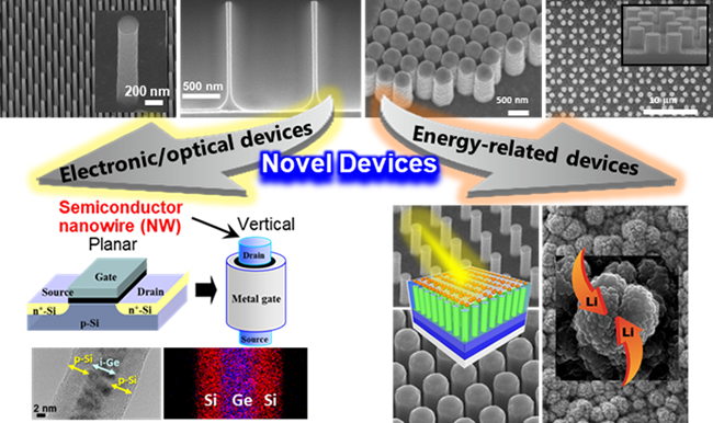
Research on fundamental properties and applications of next-generation high-speed semiconductor transistors with low power consumption, and new energy-related materials based on functionalized semiconducting nanostructures and composite nanomaterials.
Research Interests
nanowires, nanocrystals, electronic devices, optical devices, quantum effect
Assigned university/courses
University of Tsukuba Graduate School of Pure and Applied Sciences
PhD : Materials Science and Engineering
MSc : Applied Physics
Message to prospective students
We are interested in the synthesis, functionalization and characterizations of nanostructures and their use for device fabrication. Here, you can learn to apply advanced research techniques from the basics all the way to application. Let’s advance science by discovering new phenomena and creating new devices.
YAMAGUCHI Takahide
Principal Researcher, Surface Quantum Phase Materials Group, Research Center for Materials Nanoarchitectonics, National Institute for Materials Science
Research field
semiconductor, nanomaterials, surface science, superconductivity
Research outline
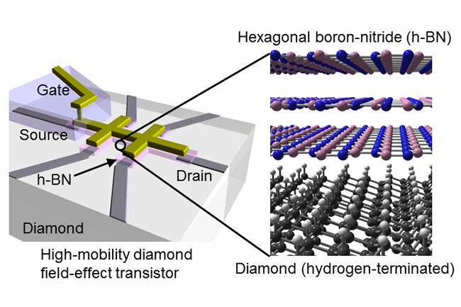
Diamond has a wide range of potential applications including low-loss power conversion, high frequency amplifications, and quantum information processing. We are conducting research on fundamental electronic properties of diamond and device applications such as two-dimensional material/diamond heterostructures for novel functionalities.
Research Interests
two-dimensional materials, heterostructure, diamond, graphene, optoelectronic devices
Assigned university/courses
University of Tsukuba Graduate School of Pure and Applied Sciences
PhD : Materials Science and Engineering
MSc : Applied Physics
Message to prospective students
NIMS has a long history of diamond research; for example, the basic model of a CVD system now widely used for diamond growth was invented in 1980's in NIRIM (former institute of NIMS). You can access advanced equipment and technical expertise for the discovery of novel phenomena in diamond and the development of new functional devices. Join us!
SHIRAHATA Naoto
Group Leader, Nanoparticle Group, Research Center for Materials Nanoarchitectonics, National Institute for Materials Science
Research field
optical materials, quantum dot, surface science, hybrid organic-inorganic materials
Research outline
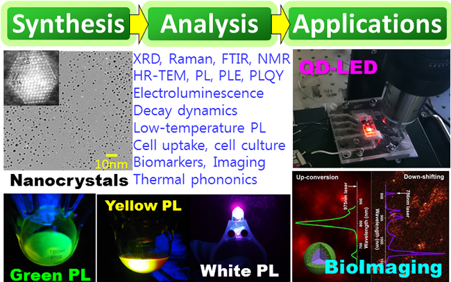
Our goal is the fabrication of innovative "light-emitting and light?receiving devices" that contribute to a safety and security based society and its sustainable development. Controlling the quantized electron state in a nanocrystal, tunable light-emitting diodes and photodiodes are fabricated. Thermal phononics is also investigated for biomedical applications.
Research Interests
nanoparticle, light emitting diode, photodiode, bio-imaging, theranostics
Assigned university/courses
Hokkaido University Graduate School of Chemical Sciences and Engineering
Materials Chemistry and Engineering Course
Message to prospective students
Students will meet various opportunities to investigate how to synthesize colloidal nanocrystals, characterize their optical performances, functionalize their surfaces, and fabricate the optoelectronic devices including light-emitting diodes. For biomedical applications, students will prepare nanocrystals adapted for cellular uptake towards theranostics.
YAMASHITA Yoshiyuki
YAMASHITA.Yoshiyuki@nims.go.jp
Principal Researcher, Nano Electronics Device Materials Group, Research Center for Electronic and Optical Materials, National Institute for Materials Science
Research field
interface science, surface science, phoeoelectron spectroscopy, synchrotron radiation
Research outline
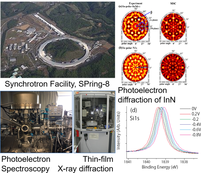
The physical property of matter is determined mainly by the electronic state and atomic structure. In our group, we use synchrotron radiation facility like SPring-8 (world's best synchrotron radiation facility), and investigate the electronic structures and atomic structures of new materials. We also elucidate static and dynamic processes of atomic structures and electronic states using operando methods like under device operation so that the nature of new materials is completely understood.
Research Interests
intetface physics, hard x-ray phoeoelectron spectroscopy, operando, interface state, power device
Assigned university/courses
Kyushu University Graduate School of Engineering
Department of Applied Chemistry
Message to prospective students
A doctor course is the most precious period to grow up rapidly as a researcher, which will be the vital foundation in your future. In NIMS, you can perform various researches with high-level NIMS scientists to be one of the world's top researchers. We recruit students who can be enthusiastic about anything.
IDE Yusuke
Group Leader, Layered Nanochemistry Group, Research Center for Materials Nanoarchitectonics, National Institute for Materials Science
Research field
catalysis, nanomaterial, environment-related materials, energy-related materials
Research outline
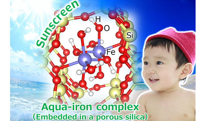
With biologically safe and earth-abundant elements, we are developing materials for possible applications in energy, environments, and healthcare. A good example is an aqua-iron complex embedded in a porous silicate that can be used as cosmetics, sunscreen, and air purifiers.
Research Interests
porous material, minerals, catalysis, photocatalysis, UV shielding
Assigned university/courses
Yokohama National University Graduate School of Engineering Science
Department of Chemistry and Life Science
Message to prospective students
Let’s develop world-wide materials with safe and secure elements!
KOZUKA Yusuke
Group Leader, Qubit Materials Group, Research Center for Materials Nanoarchitectonics, National Institute for Materials Science
Research field
thin film and interface properties, mesoscopic physics, thin film crystal growth, electronic device materials, oxide electronics
Research outline
We focus on developing quantum electronics materials. To enhance the functionality and diversity of quantum devices, we study thin film processes and nano-fabrication techniques for new semiconductors and superconductors. The devices are finally evaluated in cryogenic measurement systems. We aim to advance quantum science and technology based on materials research.
Research Interests
quantum device, nanostructure fabrication, superconductor junction, topological electronic property, ultra-low temperature measurement
Assigned university/courses
Waseda University Graduate School of Advanced Science and Engineering
Department of Nanoscience and Nanoengineering
Message to prospective students
Quantum devices are created and operated based on science and technology from various fields, such as physics, chemistry, materials science, and electrical engineering. We welcome students interested in working on quantum devices and collaborating with other researchers from different disciplines.
TANG Daiming
Principal Researcher, Functional Nanomaterials Group, Research Center for Materials Nanoarchitectonics, National Institute for Materials Science
Research field
thin film and interface properties, mesoscopic physics, thin film crystal growth, electronic device materials, oxide electronics
Research outline
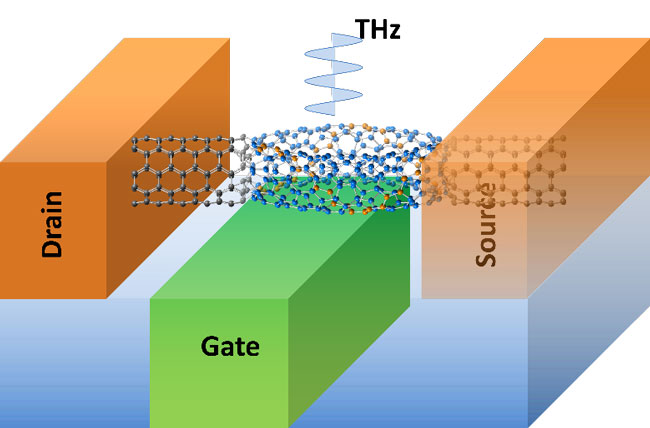
We create nano-electromechanical systems (NEMS) based on carbon nanotube (CNT) molecular junctions; elucidate the atomic mechanisms and physical properties by by advanced in situ transmission electron microscopy (TEM). We aim to apply the CNT-NEMS nanodevices as terahertz (THz) resonators and quantum sensors operating at near room temperature.
Research Interests
nanotransistors, NEMS, molecular junctions devices, carbon nanotubes, in situ electron microscopy
Assigned university/courses
University of Tsukuba Graduate School of Pure and Applied Sciences
PhD : Materials Innovation
MSc : Materials Innovation
Message to prospective students
Imagine, playing the smallest guitar (10-9 m), with the highest frequency (1012 Hz), resonating with quantum beats at room temperature. Interested in such kind of research? Let’s challenge and have fun together!
LIAO Meiyong
Chief Researcher, Ultra-wide Bandgap Semiconductors Group, Research Center for Electronic and Optical Materials, National Institute for Materials Science
Research field
Semiconductor materials, MEMS, electronic and photonic devices, surfaces and interfaces
Research outline
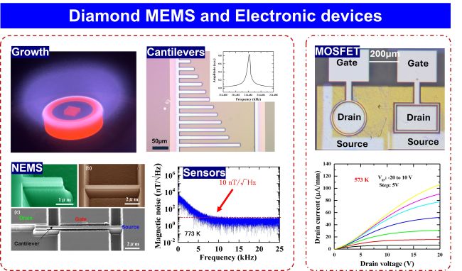
We aim to achieve extreme performance beyond the limits of conventional semiconductors through end-to-end research, from crystal growth of ultra-wide-bandgap semiconductors (e.g., diamond) to MEMS, electronic and photonic devices, and systems. By elucidating the underlying materials and devices physics, we develop ultrahigh-sensitivity, high-reliability sensors, as well as related electronic devices and integrated circuits.
Research Interests
Diamond, ultra-wide bandgap semiconductors, MEMS sensors, transistors, devices physics
Assigned university/courses
University of Tsukuba Graduate School of Pure and Applied Sciences
PhD:Materials Innovation
MSc:Materials Innovation
Message to prospective students
We harness diamond to open new possibilities in MEMS, electronics, and photonics. By bridging he disciplines of physics, mechanics, electronics, and chemistry, we tackle fundamental challenges at the frontiers of science. We welcome motivated students who are passionate about either fundamental research or translating scientific breakthroughs into real-world societal value.
TERAJI Tokuyuki
Group Leader, Semiconductor Defect Design Group, Research Center for Electronic and Optical Materials, National Institute for Materials Science
Research field
Wide bandgap materials, Quantum materials, Thin film growth, Semiconductor properties
Research outline
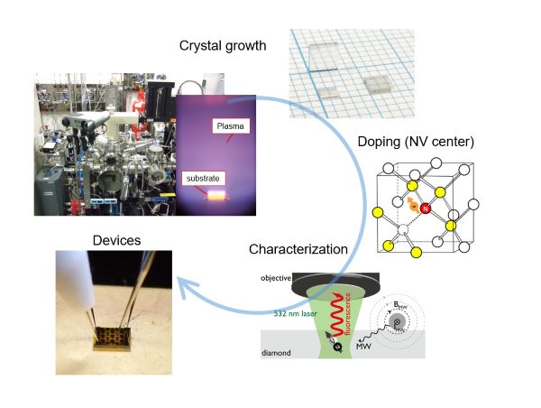
Our research interests include diamond-based quantum devices and semiconductor devices. We are developing unique crystal growth techniques and impurity doping/fabrication processes to realize quantum sensing and high-performance power semiconductor devices using NV centers, as well as to understand the underlying physical principles.
Research Interests
quantum, semiconductor, thin film growth, defect control, diamond
Assigned university/courses
University of Tsukuba Graduate School of Pure and Applied Sciences
PhD:Materials Innovation
MSc:Materials Innovation
Message to prospective students
Researchers and engineers with a broad perspective, from materials science to quantum properties, are increasingly needed in many fields. I strongly encourage you to become a leader in this emerging field.
KOZAWA Daichi
Senior Researcher, 2D Quantum Materials Group, Research Center for Materials Nanoarchitectonics, National Institute for Materials Science
Research field
Nanoscale physics, Laser spectroscopy, Chemical engineering, Magneto-optics, Quantum defect engineering
Research outline

We explore the hidden quantum properties of low-dimensional nanomaterials using advanced laser spectroscopy. By achieving atomic-level structural control through quantum defect engineering, we aim to unravel the mysteries of light-matter interactions at the nanoscale and create innovative material platforms for next-generation quantum technologies.
Research Interests
Quantum nanostructures, Low-dimensional semiconductors, Solid-state quantum light sources, Magneto-optical materials, Organic color centers
Assigned university/courses
University of Tsukuba Graduate School of Pure and Applied Sciences
PhD:Materials Innovation
MSc:Materials Innovation
Message to prospective students
Nanostructures hold profound mysteries that go beyond our intuition. Join us in the excitement of unraveling these secrets and shaping the future of quantum technology together. We seek passionate individuals to integrate physics, chemistry, and mathematics to explore the new frontiers of physics as a team.