About Semiconductor Functional Device Group
Development of multi-functional electronic devices beyond von-Neumann architecture
In association with the drastic progress in AI technology, improvements of semiconductor device performance have been endlessly demanded. To keep up with these trends, many requirements, such as downsizing and high integration density of the transistors, electric power saving and high-speed processing, must be satisfied. Therefore, novel arithmetic circuits beyond von Neumann type architecture are highly required besides reformation of the current Si-based CMOS devices. The main challenge of our group is to establish innovative device operation mechanism based on the concept of nanoarchitectonics of molecular and two-dimensional materials to transcend the limitation of modern Si technology.
Specialized Research Field
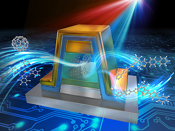
Multi-functional tunneling transistors with molecular quantum dots
Based on a fundamental concept that organic molecules are excellent quantum dots, we have been developing multi-functional tunneling field-effect transistors (TFETs). Here, quantum characteristics of nanoscale organic molecules facilitate various carrier tunneling behaviors in the CMOS compatible architectures. Optically controllable TFET with photochromic molecules [1], multi-level tunneling through molecular orbitals of multiple phthalocyanine molecules [2] and TFET with radical molecules for novel spintronic devices have been developed [3].
References
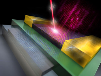
Molecular nanoarchitectonics for multi-functional organic field-effect transistors
We have been paving the way in organic electronics by exploiting distinct features of anti-ambipolar transistors (AATs). AATs make it possible to control increase as well as decrease in drain current, demonstrating negative differential transconductance (NDT). By taking advantage of such uniqueness, a variety of nanoelectronics devices beyond von-Neumann type architectures, such as multi-level logic circuits [4, 5], logic-in-memory [6, 7], reconfigurable two-input logic gates [8] and artificial synaptic devices [9] have been developed.
References
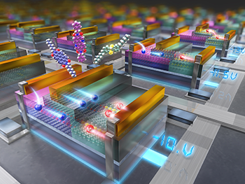
Two-dimensional materials nanoarchitectonics for beyond Neumann type device architectures
Cutting-edge transistor structures have been further complicated by adopting two-dimensional nanosheets as transistor channels. Then, 2D-layered materials, such as graphene and transition metal chalcogenides, are expected to be incorporated to go beyond the limits of von-Neumann type architectures with current Si technology. We are developing multi-functional FETs: multi-valued optical memory [10], reconfigurable two-input logic gates [11] and neuromorphic devices [12], based on the nanoarchitectonics of 2D heterostructures. These novel electronic devices are expected to contribute to the drastic increase in integration density, remarkable reduction in power consumption and ultra high-speed processing.
References
Group Members