Future Quantum Society
日本語
Materials Science × Quantum Material
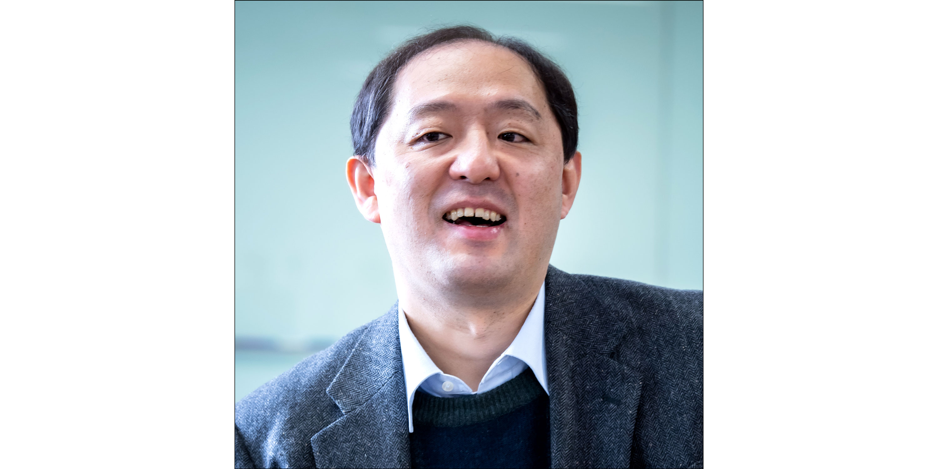
Yutaka Wakayama, Deputy Director/Administrative Director, WPI-MANA
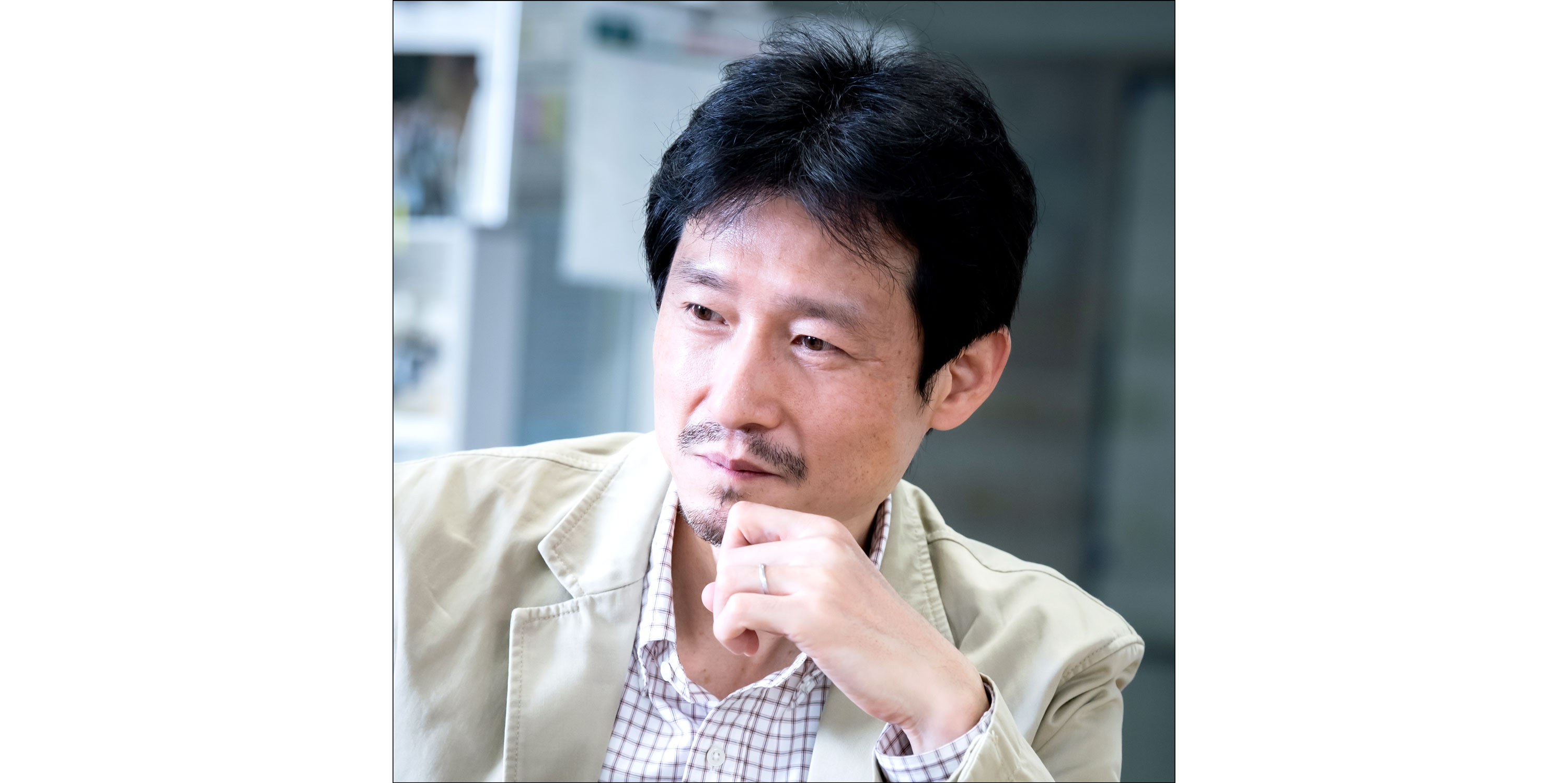
Takayuki Harada, Independent Scientist, WPI-MANA
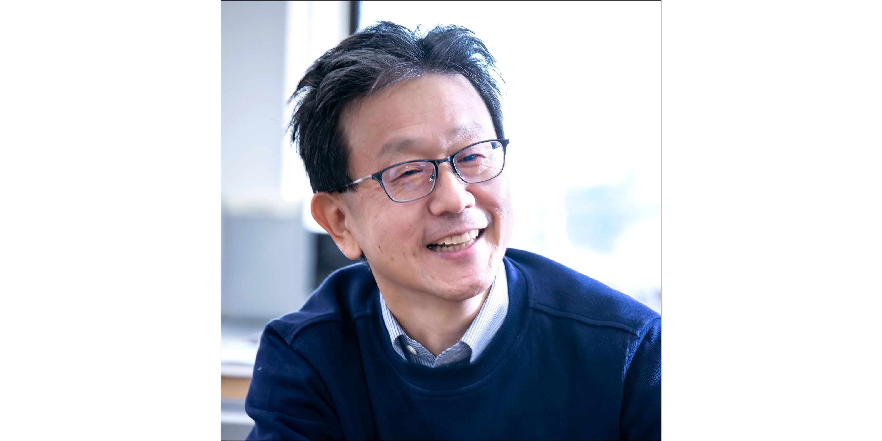
Takafumi Sato, Professor/Principal Investigator, WPI-AIMR
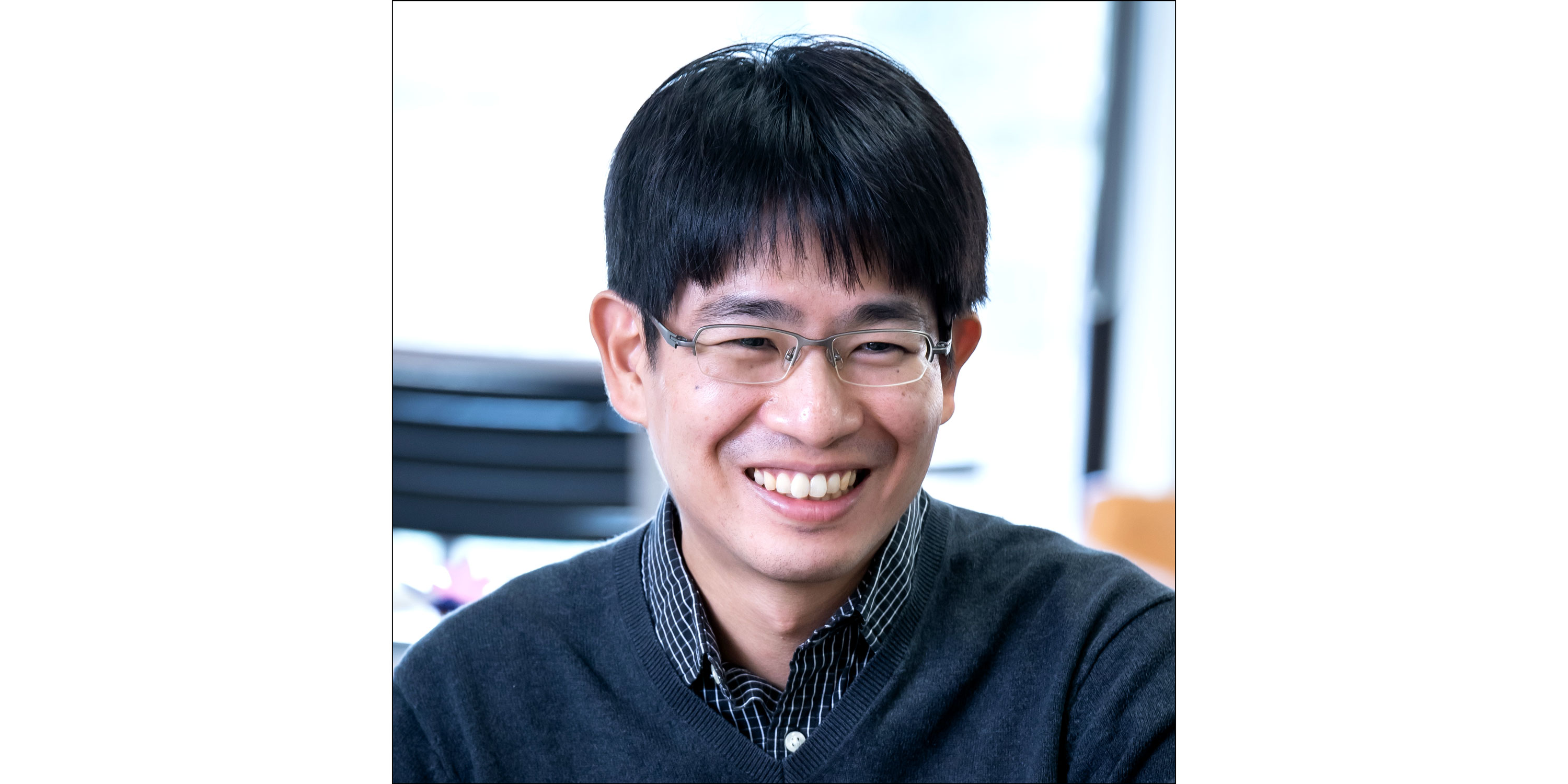
Akichika Kumatani, Associate Professor, WPI-AIMR
Hirofumi Oka, Assistant Professor, WPI-AIMR
Devices that support the coming future quantum society can be fabricated from unknown materials. New discoveries by materials scientists will be the key to “quantum materials” that support the foundations of our future. Therefore, in this WPI round-table discussion, we had materials scientists from WPI-MANA and WPI-AIMR (Advanced Institute for Materials Research, Tohoku University) discuss the current status and prospects of quantum materials. Researchers continue to explore the invisible nano world while thinking about unknown materials that emerge from various “individual characteristics of materials.”
− In its Quantum Technology Innovation Strategy, the Japanese Government has listed quantum technology fields, such as quantum computers, quantum software, quantum communication/cryptography, and quantum measurement/sensing. Moreover, the government has positioned the establishment of research and development as well as supply infrastructure for quantum materials as important missions. Quantum materials, as defined by the government, are materials that exhibit high-performance quantum functions. Therefore, today, I would like to ask each of you about the relationship between your research and quantum materials. First, please tell us about your research field and theme.
Wakayama: My specialty is organic electronics. My research involves the exploration and proposal of new functions and operations of transistor-based devices. Organic transistors are being researched by various researchers, but I would like to pursue my own themes to the extent possible. I am working so as not to get entangled in too much development competition.
Yutaka Wakayama, Deputy Director of MANA
Harada: My research is focused on thin film heterostructures. Joining thin films of different crystals reveals physical properties that are more than just the sum of their parts. There are many heterostructures around us, and semiconductor devices are also a cluster of heterostructures. I would like to create heterostructures that nobody has ever created.
Sato: My specialty is on advanced spectroscopy measurements. My research involves the use of a photoelectron spectrometer to irradiate lights onto the material surface and precisely measure the emitted photoelectrons. We are developing world-class equipment to measure graphene, superconductors, topological materials, and others.
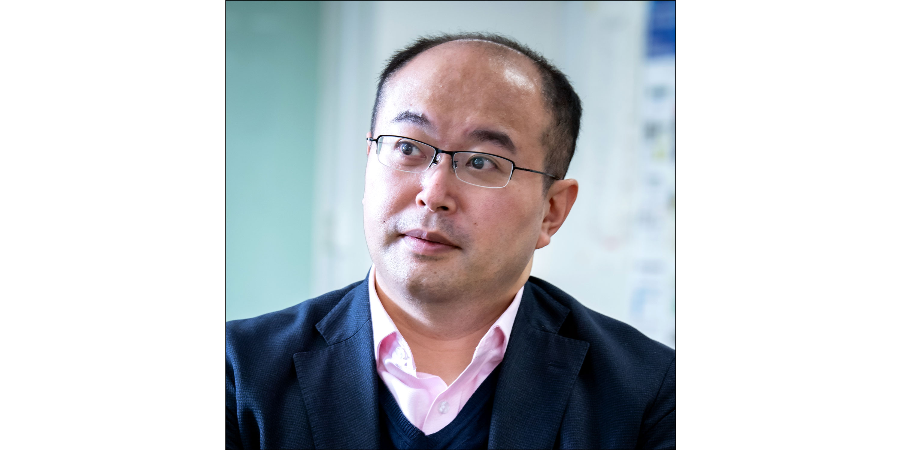
Kumatani: My specialty is also on advanced measurements. My fascination lies in the “interface,” where materials come into contact with each other, and we are currently making a scanning electrochemical microscope (SECM) to perform electrochemical analysis to observe the ions (de)inserting through the battery interface. I am also affiliated with both WPI-AIMR and WPI-MANA under a cross-appointment system.
Oka: My research involves the use of an ultra-low temperature scanning tunneling microscope (STM) to examine materials down to the atomic scale. Materials have completely different properties at the atomic scale compared with those at the macro scale. I am particularly interested in magnetism and superconductivity in my ongoing research.
Impressions from the term “quantum material”
− What are your impressions of the term “quantum materials” from your respective research perspectives?
Sato: As a condensed matter physicist, I feel that the term “quantum materials” has a very broad meaning. If a material that has quantum effects occurring in its physical properties is called a quantum material, then most of the materials that I measure would fit under this classification. There is no consensus on the definition of this term.
Wakayama: In society, I think it starts from the question, “what is a quantum material?”. Today, there are many words that include the term “quantum,” such as quantum computers, quantum communication/cryptography, and quantum software. It also appears in TV commercials. There is a wide range of words with the term “quantum” added as prefix. In addition, the government’s plan is to address these at a Japan-wide level. What can we do in this context? I think it is ultimately with materials. For example, materials scientists present the discovery of this new function or such in graphene.
Harada: The term “quantum material” is a word that emerged from the recent expectations toward quantum technology, making the definition somewhat loose. The definition is also likely to change in the future. When thinking about the relationship with my research, I have the impression of quantum materials being “things with peculiarities,” such as superconductors and topological materials. Heterojunctions of one thing with the peculiarities of another thing created yet another material with even more peculiarities. That is my impression.
Takayuki Harada, Independent Scientist of MANA
Kumatani: When I hear the term “quantum material,” I think, in general, people will consider two-dimensional (2D) materials. 2D materials consist of atomic structure coordinated on an ideal two-dimension. They have effects, such as interfacial conduction. I think this is common among the five people in today’s round-table discussion.
Wakayama: The classification of “quantum materials” may have implications for the dissemination of the concept to the general public. It is similar to how the term “topological” frequently appears in the field of materials science these days.
Sato: I think it is a good thing in terms of dissemination.
Wakayama: Twelve year ago, when Kyushu University’s WPI-I2CNER (International Institute for Carbon-Neutral Energy Research) incorporated the term “carbon neutral” into its name, the term was not recognized by society, but now everybody knows this term. I think this is an example of how a keyword leads society. I believe that the term “quantum” will also lead society in the future.
Oka: My research focuses on what happens when materials are gradually reduced in size from the bulk to the single atom. I think one of the boundaries of the change in materials properties is where the quantum effect becomes dominant. People generally consider electrons as “particles,” but they also behave like “waves.” And this wave-like behavior of electrons becomes evident in the regime where the quantum effect appears. Scanning tunneling microscopy can visualize these electron waves. Therefore, I have always thought that the materials that I have investigated are quantum materials, but it seems that the quantum materials that the government is thinking of are materials that exhibit physical properties that are different from conventional ones, such as graphene and topological insulators.
- By listening to everybody’s stories, I get the feeling that what materials scientists think of as quantum materials are two-dimensional materials, such as graphene and topological insulators. What is at the forefront of this type of research today?
Sato: For example, a new research trend of graphene as a two-dimensional material is the investigation of new physical properties by contacting two pieces of graphene sheets with a small angle mismatch by e.g. one degree. Such degrees of freedom, like twists and shifts, are unique to two-dimensional materials, and they cannot be done with ordinary three-dimensional materials. These degrees of freedom were hardly explored, and the combinations are infinite. I believe that it is the hottest trend.
Takafumi Sato, Professor/Principal Investigator of AIMR
Wakayama: This is the “magic angle.” It was a shocking idea that was akin to the Egg of Columbus.
Sato: This is the research result that surprised me the most recently.
Wakayama: A researcher commented that “it should be this way” theoretically, and it immediately attracted attention once an experimental scientist achieved it. It has only been 12 years since André Geim and Konstantin Novoselov were awarded with the Nobel Prize for graphene. However, the field is steadily expanding with the emergence of two-dimensional materials for semiconductors. I think that a “change of mindset” is important. Superconductivity is consistently aimed at room temperature, but quantum computers are based on the idea of working at low temperatures. Technologies that can measure at low temperatures, technologies that can move elements at low temperatures are needed. We are also seeing the possibility of actual development.
Sato: Technologies include “technologies that are disseminated worldwide” and “specialized technologies,” such as quantum computers. Not every household needs a quantum computer.
Wakayama: However, materials scientists should be aware of quantum-related problems in their research. Specialists in quantum technologies say that “the material is the ultimate aspect.” If you are making something so small that quantum effects appear, then you always encounter the problem of structure, such as crystals.
Initiatives originating from collaborative research
− Joint research in adjacent and different fields is essential for innovation.
Kumatani: There are some cases where the research being conducted at WPI-MANA is connected to the electrochemistry-related research that I am doing under a microscope. For example, the electric double layer transistor that Dr. Harada is working on. The phenomenon of the electric double layer in electrochemistry can be applied in physical property research. Additionally, the topic of two-dimensional materials, where the material is twisted by one degree, came up earlier. However, I think that I can re-import such materials into my research subjects. I would like to attempt various things, such as 2D materials with different angles. To begin with, 2D materials are generally clean. However, I have recently felt that a clean structure does not necessarily directly lead to the improvement of electrochemical reactions in my field. In Dr. Wakayama’s laboratory, two-dimensional materials with large areas and more surface defects than usual can be created. In terms of electrochemical reactions, those methods produced better results.
Wakayama: When I first started making large-area two-dimensional materials, even when I tried to evaluate transistors, it was completely useless. I thought that I could only make low-quality ones with many defects. After hearing that catalytic reactions were good with only defects at the edges and that they were advantageous in terms of catalytic reactions, I asked Dr. Kumatani to evaluate it. This was a joint research where I synthesized thin films and Dr. Kumatani measured them.
Kumatani: Furthermore, defects in these materials can now be controlled using scanning electrochemical microscopy.
- Does this mean that the number of defects can be increased by operating the microscope?
Kumatani: That is correct. One of scanning electrochemical microscopies can make detects via an electrochemical reaction by creating an electrolyte “droplet” between a probe (needle) and an object. The material can be scraped with that droplet.
Akichika Kumatani, Associate Professor of AIMR
Sato: Does this mean that etching (microfabrication in semiconductors, etc.) can be done?
Kumatani: I think that this is essentially micro-scale etching. Elements can be scraped with droplets. For example, the goal is to create a catalyst with more defects when wanting to create a large-area two-dimensional material, but I think you want to know how many flaws it takes to stop the process. The idea is to take it to the limit. I would also like to know how much we can increase the area of a two-dimensional material that has only one layer at the atomic level without any defects.
Sato: If made properly with molecular beam epitaxy (MBE), then something considerably clean can be made.
Harada: MBE is a method of making a thin crystal film by ejecting atoms in a clean vacuum and adsorbing them to a substrate.
Wakayama: Two-dimensional materials can be made into large areas through chemical vapor deposition (CVD) and MBE. We have to properly test and investigate the degree by which the defects mentioned by Dr. Kumatani increase, or it will not lead to implementation.
Harada: Speaking of joint research, when I was in Tohoku University, a heterojoined thin film was evaluated by Dr. Sato’s angle-resolved photoemission spectrometer. As my specialty is thin-film growth, I often collaborate with researchers skilled in advanced measurements.
Sato: With photoelectron spectroscopy, we can investigate how electrons, which determine the properties of thin films, behave in solids. Actually, some thin films fabricated in our laboratory have been measured by Dr. Oka using the STM technique, besides the photoelectron spectroscopy measurements in our laboratory.
Oka: Photoelectron spectroscopy makes it possible to investigate how electrons move in materials, while scanning tunneling microscopy allows for the investigation of more localized electronic states.
Sato: There is a complementary relationship between the photoelectron spectroscopy and scanning tunneling microscopy. Scanning tunneling microscopy observes the states in real space, whereas photoelectron spectroscopy observes the states in a “reciprocal lattice space.” By complementary utilization of the two techniques, the whole picture of electron behavior in solids can be obtained.
Breakthroughs by surpassing conventional technologies
Wakayama: Moreover, the biggest problem with current supercomputers is that they consume too much power. Back in the day, there was lots of talk about having to be number one. However, now people talk about having to be number one while reducing power consumption. Significant power consumption reduction requires great changes. Quantum materials are possible candidates for bringing about such change.
Sato: Current computer technologies are silicon-based but their limits are already known. Making a breakthrough in the energy conservation problem requires materials scientists developing quantum materials that have not received much attention to date. It is also important to demonstrate useful materials that can be implemented to society, while receiving feedback from quantum technologies.
Wakayama: Limits on the miniaturization of silicon will be eventually reached. There is recent news that 2-nm chips will be mass-produced. Two nanometers. I do feel that we are approaching a limit.
Sato: The smallest unit is the atom. Once you are at the single-atom scale, then the atomic-level technologies that can be done with silicon stop. However, current silicon technologies are truly incredible, and even if a new material comes out, it will not be a sudden replacement. It will be a gradual change over the course of 10–20 years.
Harada: Silicon has a long history, and its properties has its own merits.
- Is it necessary to escape from the silicon world in order to make a breakthrough?
Harada: If it is an extension of the current computer, then it will probably continue with silicon. However, if a computer with different principles appears, then it can be a different material.
Sato: In that sense, regardless of national policies, I think that materials scientists should try their hand on various topics, with the awareness that they would not know whether it will be usable, but to try it regardless.
Wakayama: That is how we expand our possibilities. However, for any technology to reach the level of social implementation, a manufacturing method must be established, and mass production must be achieved.
Harada: There are indeed various stages leading up to social implementation. The first transistor started as “putting a needle on a germanium stone,” but it would have been impossible to imagine the world today, where semiconductors have developed and become widespread. A long period of time and a wide range of channels are needed from discovery and development of functions to its social implementation. The expansion of possibilities is that more people enter the market. If the term “quantum materials” becomes permeated to the extent that even elementary school students know it, participation of various people in different fields will be expected.
Oka: There are various stages in research on quantum materials. If we can fabricate high-quality materials using the MBE method, then, although it is difficult to fabricate them with large area, we might be able to discover materials properties promising for future applications. This is my motivation. Researchers work at various research stages and have their own motivations. One breakthrough at a research stage leads to breakthroughs at other research stages. And successive breakthroughs can achieve the implementation of materials in real devices.
Hirofumi Oka, Assistant Professor of AIMR
Sato: Dr. Oka’s motivation is a general way of thinking of a basic researcher.
Oka: I think there are many researchers who are working on materials that might be implemented in real devices in the near future. However, researchers must overcome various obstacles before implementation. This is why no one knows what material will replace silicon. I think that one important factor is the “coincidence” that successive breakthroughs occur at various research stages.
Sato: Expanding the network of researchers is important for creating a series of breakthroughs. In general, since researchers only see their own research phase, the creation of exchanges among basic science, application, and implementation fields would be useful to trigger breakthroughs. Individuals who have a bird’s-eye view of these fields are also important.
Harada: The current data-driven research is a field that is close to such hub concept. There have been databases of the crystal structure of materials, but the electronic state has recently become a database as well. There is a number of information to choose from when creating a new thing.
Sato: In terms of exchanges in each field, WPI-AIMR provides opportunities for researchers to gather and discuss. I think that WPI-MANA is in a similar situation.
Kumatani: In terms of connecting researchers, I have a cross-appointment between WPI-AIMR and WPI-MANA. This is because my research area spans in both organizations.
Wakayama: Tohoku University and NIMS have cross-appointments, and there are currently 10 people involved. Dr. Kumatani is one. However, because a system is in place does not necessarily mean that connections will be created. My collaboration with Dr. Kumatani also began when we met at a symposium in France in 2018 and chatted.
Kumatani: This was the European Materials Research Society (E-MRS) 2018 Spring Meeting.
Wakayama: I think that it is not enough to do things online.
Oka: Chatting with other researchers after meetings is very important. For example, when a friend of mine introduced his/her friend to me and we had a chat, we found unexpected research interests that we have in common.
Nurturing something new over the years with love
- Our time here is coming to an end. Lastly, I would like to ask everyone to share their thoughts and impressions regarding materials science and its appeal.
Wakayama: I occasionally go to the university to give lectures, and I always talk about my experiences as the last message of my lectures. About 30 years ago, I worked for a glass manufacturer. It was a development team for liquid crystal displays. At the time, CRT displays were still the norm. Liquid crystal technologies were only used in wristwatches and calculators. I could not believe that LCD screens would become TV screens, but it was when my boss would tell me, “Let’s think about the post-LCD era!.” Hence, I started organic EL research. Then, LCDs were achieved, and now the organic EL display is also realized. In addition, LCD TVs and organic EL TVs line the fronts of electronics shops. Developing something takes about that much time. A time scale of approximately 30 years. That is why the right time to start is when people say that it cannot be done. This is also the case for quantum materials. It should be started now. Thirty years from now, people will be saying, “with graphene, in the beginning, we used to make them by sticking scotch tape on them and peeling them off.”
Harada: It certainly is the case that a long time scale is needed to achieve social implementation. However, in the sense of “trying out small ideas,” materials sciences allow for rapid research. In my case, I think about what kinds of crystals I can combine, and I try it immediately. It is almost like a puzzle. If that puzzle fits well, then social implementation may eventually arrive. Materials science has that kind of appeal.
Sato: I think that materials science is a field that creates new things that originally did not exist in the world, i.e. create something from nothing. I believe that is the real pleasure for materials scientists. Personally, I feel happy to do such creative things. Ultimately, I think that we cannot continue doing research without being surprised and excited.
Wakayama: I agree. I think that WPI-MANA plays an important role in NIMS with regards to creating something from nothing.
Harada: Raising the properties of a material 2 or 3 times instead of just 10% leads to breakthroughs. I do not think you can double or triple something without changing your way of thinking. It is this change in thinking that creates something new.
Kumatani: I believe that materials science is an interdisciplinary field that is made up of various fields. Its interdisciplinarity and diversity is the driving force behind the creation of new things.
Oka: When a small amount of iron or cobalt is deposited on the same substrate, they look very similar, but their physical properties are completely different. Materials have individual characteristics that cannot be determined by their macroscopic appearance. Even invisible materials have their own individual characteristics. Finding the individual characteristics of materials is interesting to me in materials science.
Sato: Materials scientists admire the individual characteristics of materials. For example, pursuing something unusual. There must be something interesting regarding that endeavor.
— The interview took place at AIMR Main Building, Tohoku University on 25 November 2022. —
— Texts by Osamu Shimizu, Academic Groove. —
#####
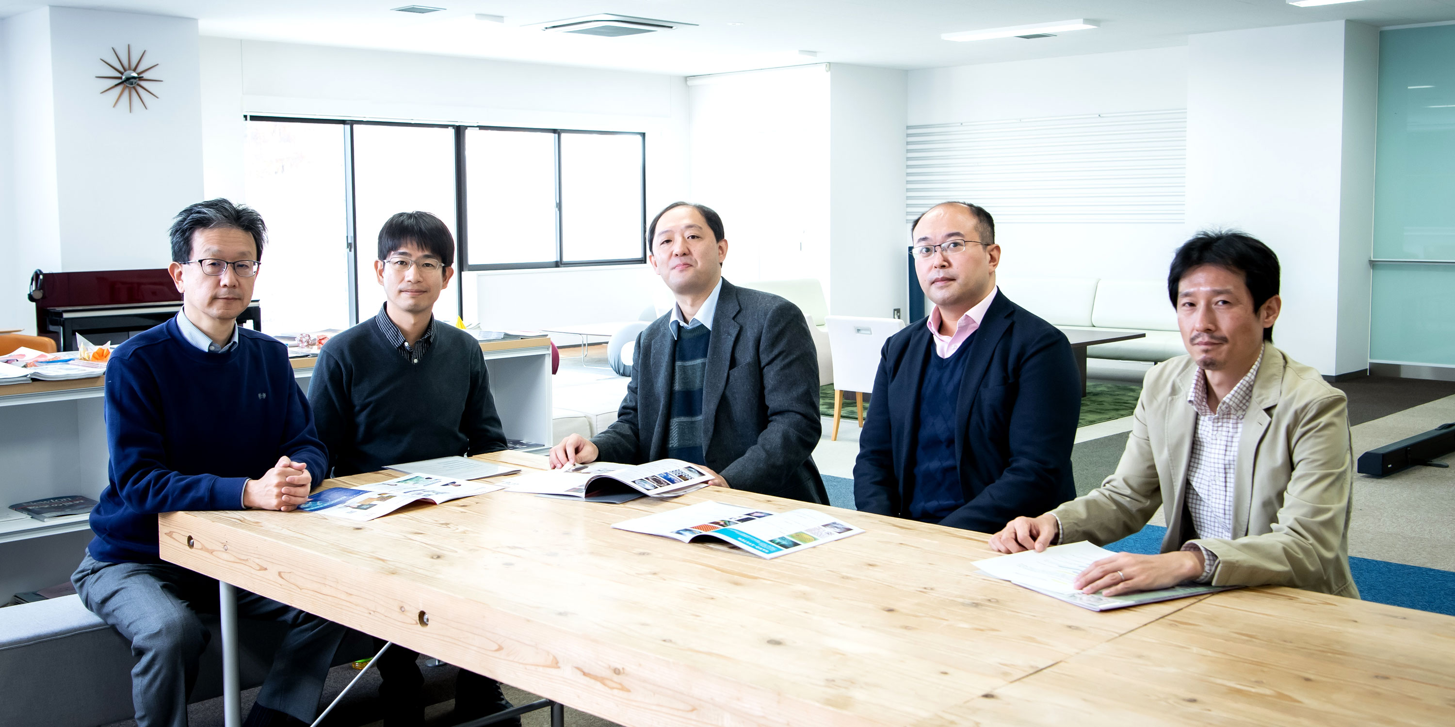
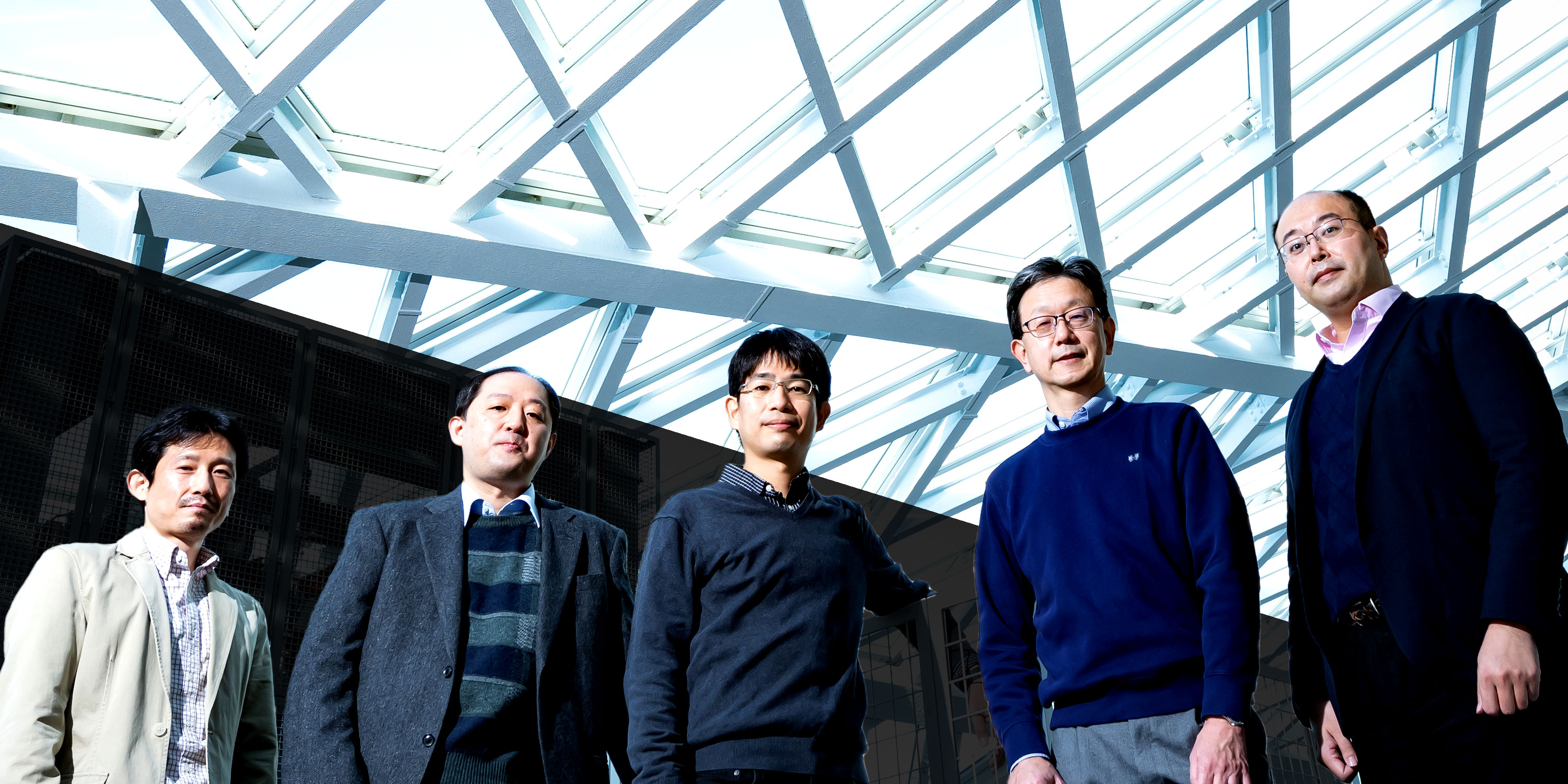
(From left) Dr. Wakayama, Dr. Harada from MANA, Dr. Sato, Dr. Kumatani, Dr. Oka from AIMR
“Quantum materials and WPI-MANA”
Since 2020, the Japanese Government has formulated and released the Future Quantum Society Vision, which is an imagined diagram of the future created by quantum technology, and the Quantum Technology Innovation Strategy, which is the roadmap to realize this vision. Additionally, with the National Institute for Materials Science (NIMS) being designated as one of the quantum technology innovation bases, WPI-MANA is now taking steps toward the realization of quantum materials. The future created by quantum technologies begins with materials.
Tohoku University
Advanced Institute for Materials Research (AIMR)
Advanced Institute for Materials Research (AIMR) was established at Tohoku University in 2007 as one of the first five centers of the World Premier International Research Center Initiative (WPI). The institute aims to form a world-leading materials science research center in an outstanding environment, by bringing together leading researchers in physics, chemistry, materials science, bioengineering, electronics, and mechanical engineering.
Further information
World Premier International Research Center Initiative (WPI)