“Be as lucky as possible!
The Go-To Guy for Ultra-Pure hBN Crystals
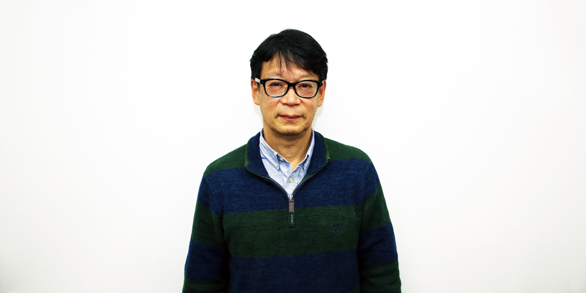
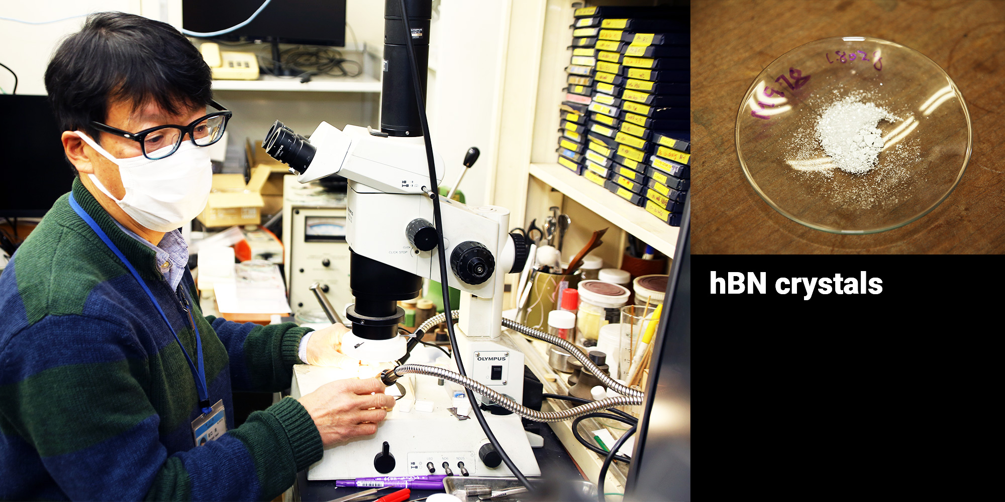
Takashi TANIGUCHI
NIMS Fellow, Project Leader of the Quantum Materials Project
Dr. Takashi Taniguchi is renowned for high-pressure synthesis of hBN (hexagonal boron nitride) crystals, a key material in nanotechnology research. His ultra-pure hBN crystals are the highest quality available, and they have been attracting the attention of researchers around the world, contributing to a variety of research into two-dimensional materials in the fields of quantum physics and quantum devices, including graphene research.
Dr. Taniguchi joined MANA in April 2020, and is now the leader of the newly launched NIMS Quantum Materials Project.
Crucial Material for Quantum Research
− You’re world-famous for your hBN crystals. Why are you the go-to guy for this material?
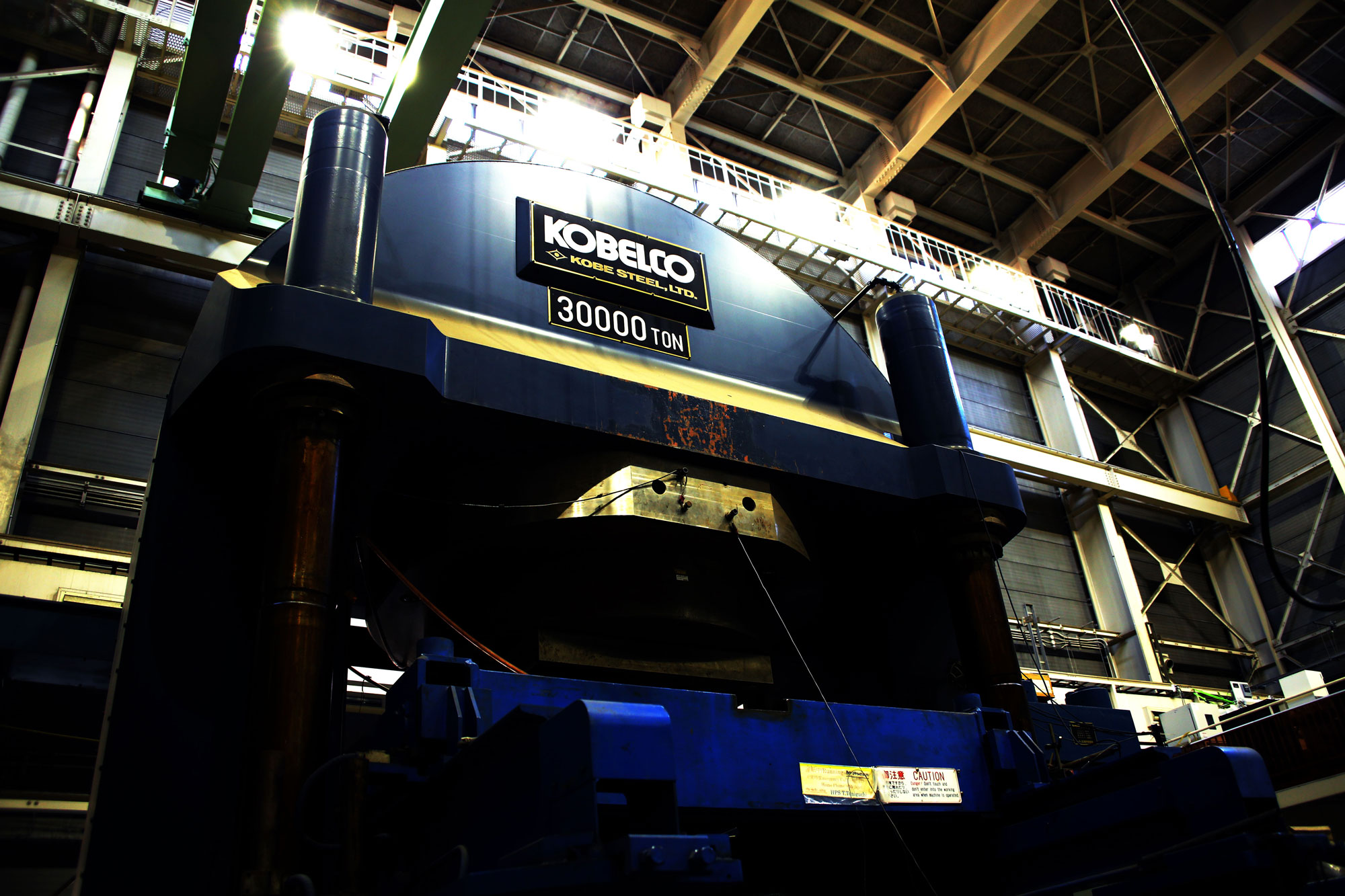
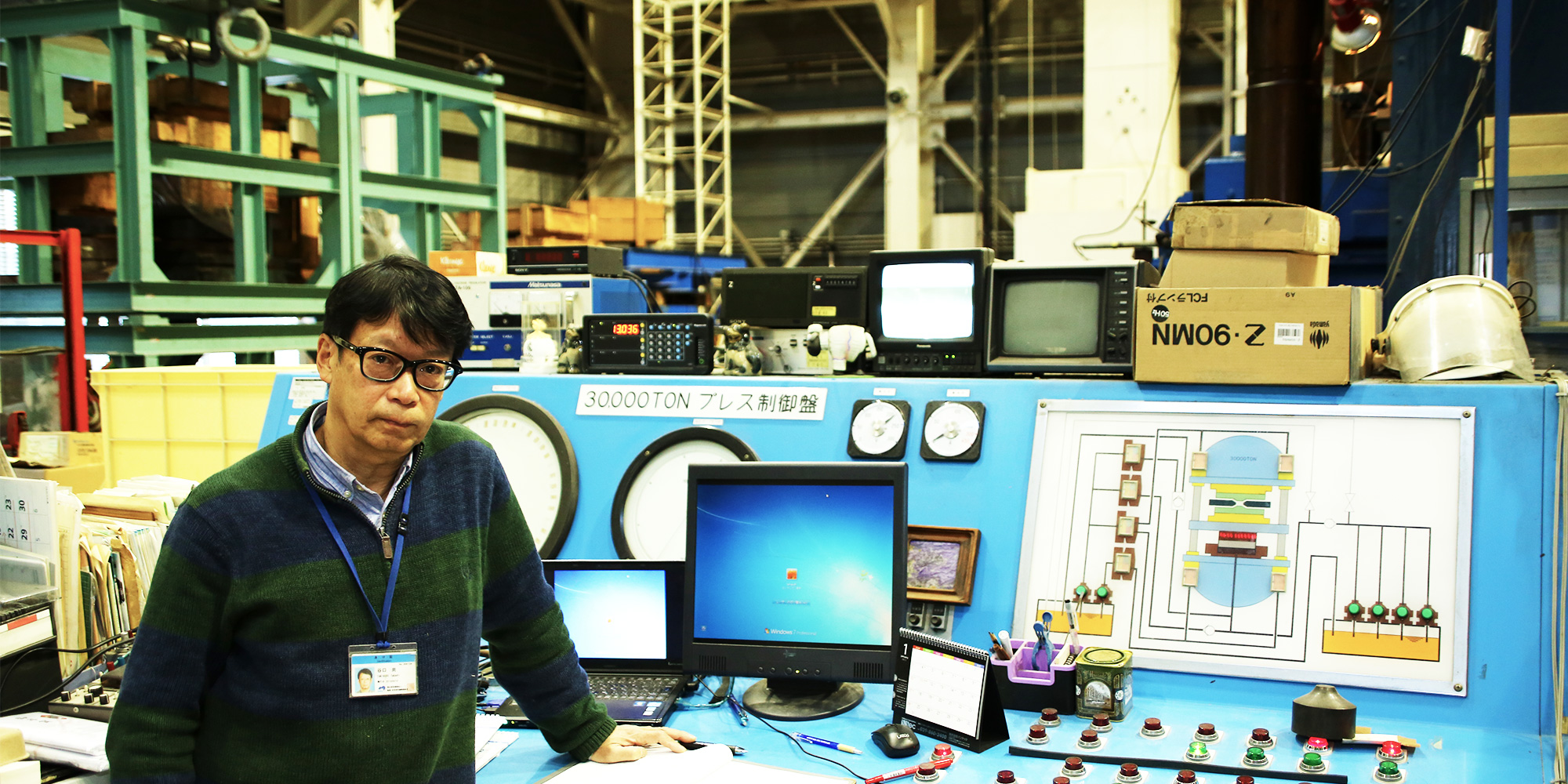
Mostly it’s just a result of luck and good circumstances, especially having access to our beautiful 30,000-ton hydraulic press. But more importantly, for more than 10 years I have had the freedom to concentrate on this work, to keep the momentum and direction, using very nice facilities. Being able to monopolize the equipment is a huge benefit -- such a situation is not easy to come by.
I have been studying single crystal growth under high pressure for more than 20 years now. High-purity crystals can be obtained using facilities like these, including our press, and I have sole use of them.
Also, as a NIMS researcher, I have a big advantage over university people -- no lecturing responsibilities -- and that frees up a lot of time, which I can put into my research. Of course, this is a national lab, so there are some big projects I participate in. But there's also freedom to do other things of interest.
− What are the crystals used for?
They’re mostly used by researchers studying graphene. As you probably know, graphene is a monolayer of graphite, a single layer of carbon atoms arranged in a two-dimensional hexagonal lattice. It conducts electricity and heat with impressive efficiency, so it is being used in quantum transport research, and we expect lots of applications, including anti-corrosion coatings, sensors, electronics, flexible displays, solar panels, DNA sequencing, drug delivery -- all kinds of things.
But producing graphene of decent quality, and in large quantities, is extremely difficult, and so is handling it. The problem is, it's very sensitive -- the atomic monolayer interacts with whatever substrate it’s on, so the graphene surface allows no free bonding, and the carriers can’t move smoothly. You need an insulating layer, a perfectly flat, protective substrate that won’t interfere with the graphene’s electrons, and for this hBN crystals seem perfect. They have almost the same structure as graphene, and they don't bond. But they do insulate -- that is crucial.
Originally, my main focus was cubic boron nitride (cBN) crystals, and I achieved a high level of purity by using high pressure. High-purity hBN crystals were also there in my sample capsule when I took it out of the press, as a byproduct. Then, one day, my colleague Kenji Watanabe noted that since they were almost colorless and very transparent, the optics people might find them interesting.
There were some impurities, which imparted a yellowish or brownish tint, but if the crystal is clear, that doesn’t matter. So we published some papers on single-crystal hBN. A while later, graphene was discovered, and those researchers took an interest.
They knew hBN should be a good substrate for graphene, and they tried to use it. But commercially available crystals were very small, like powder, 5-10 microns, and they didn’t work so well. Then they found our NIMS paper on bigger hBN crystals and the collaborations started.
− What is the relevance of your research to nanoarchitectonics?
The crystals can be used to study very precise things, to manipulate things at extremely small scales, like electrons and so on. Each crystal is only 1mm, but that’s still useful for graphene research. At the 10 or 100 micron device scale, they are big enough to realize some physics results. The field is moving very fast -- when I started this work five years ago, there was very little of this work going on. But nowadays it is highly advanced technically.
Encouraging Collaboration Worldwide
− Your crystals must be very expensive to make. Why do you supply them free of charge?
It's a two-way collaboration. We supply them for free, but in exchange we get material evaluation agreements with institutions and universities, as well as being included in papers.
In the beginning, some Columbia University researchers published a paper with us as co-authors, and it was quite sensational in the field. After that, many requests arrived, and we supplied them, too. So we just continued that way, with collaboration.
It has been suggested that we change our strategy to a payment basis, but if we did that, the collaborations would end. As it is, people include us as co-authors of their papers, totaling more than 1,000 so far, and this raises the profile of NIMS. Furthermore, collaborators have given us useful feedback to improve the quality of our hBN crystals. So collaboration is better for everyone.
− Where do you go from here?
One important thing is to figure out some alternative way to make the hBN crystals without using this huge apparatus, and also make them bigger, which would be a great benefit for research.
But so far, the chemistry is not well controlled without pressure, which is why we need the press. There have been some attempts elsewhere, but as far as I know, no one is catching up in terms of crystal quality. Without the press it would be much more difficult.
Nanosheet technology will have a role. This is a very sophisticated area at MANA, and some people are making good functional nanosheets without having to use high pressure. Nanosheets are not perfect for quantum manipulation, as the orientation is a bit random, but they have other important functions.
− Could you tell us about your new position with NIMS’s Quantum Materials Project?
The government has selected a number of priority research projects, and is directing funds toward them. One is quantum technology -- quantum computing, quantum information and so on -- related to the very small physical world, the quantum domain.
We need to study the fundamentals of the materials themselves, how to combine them with other materials, how to make interfaces, etc. This kind of work is being done in many places, including RIKEN, the University of Tokyo and others, and many institutions are collaborating. So the president of NIMS proposed a new research plan centered around quantum physics.
Quantum research needs everything -- the materials, modeling, theory, equipment and so on. NIMS can play a key role in materials, so we started the Quantum Materials Project last year.
Good Life = Good Research
− What can you tell young researchers about the future of materials science in general, and your field in particular?
Well first of all, as I mentioned, I'm a very lucky guy, because I have access to excellent facilities, which is a huge advantage in my research. So I would say to young researchers: “Be as lucky as possible!” But seriously, you can’t know the future, though you can be ready to be lucky -- you can be prepared for when good fortune comes along.
The most important thing is to enjoy the work. I want to emphasize that my main interest is in things that nobody has done before, and this is what makes my work so exciting. Naturally, we are responsible for explaining our work to get taxpayer funds and so on -- that’s the situation anywhere. But still, enjoy the work, and love what you do. If life is good, so is the research.
#####