Pioneering development of in situ transmission electron microscope techniques for direct property measurements on nanoscale materials
D. Golberg , N. Kawamoto , M. Mitome , Y. Bando
State-of-the-art in situ analytical methods of nanomaterial property measurements inside a high-resolution transmission electron microscope (TEM) were for the first time designed and implemented for mechanical, electrical, thermal, optical, optoelectronic, and cathodoluminescence characterizations of various nanoscale nitrides, oxides, sulfides, selenides, phosphides, and carbides. Clear atomic structure–functional property relationships were established, which is the “Holy Grail” of the material “nanoarchitectonics” concept and the entire material science field.
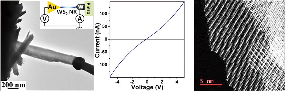
Unprecedentedly high spatial (down to 60 pm), energy, and temporal resolution capabilities, only achievable in the most modern high-resolution TEMs, were greatly enriched by adding new possibilities for delicate nanomanipulations (with precision better than 1 nm) and electromechanical, thermal, and optical probing of diverse nanostructures using piezo-driven stages and optical fibers inserted into a TEM column. Temperature gradients along and across carbon nanotube electrical interconnects under resistive heating were elucidated for the first time[1]. The quantitative kinetics of the famous Nobel Prize-winning “Scotch tape” technique for making graphenes, and of various inorganic atomically thin nanosheets in booming layered semiconductors were fully understood, taking the example of molybdenum disulfide single-crystal direct nanoscale peeling in a TEM[2]. Young’s modulus, tensile strength, and fracture toughness of carbon, boron nitride, and tungsten disulfide nanotubes and nanosheets, and silicon, zinc oxide, and sulfide, and gallium nitride nanowires were directly and unambiguously measured for the first time[3]. World-first in situ TEM optoelectronic and photovoltaic tests of the most popular optical materials, e.g., cadmium sulfide, titanium oxide, zinc oxide, silicon, and various perovskites, were performed and specific optoelectronic characteristics were completely understood in terms of their nanomaterial local crystallography and atomically and chemically resolved interfaces, as well as defect structures.
Main Papers
- “Direct imaging of Joule heating dynamics and temperature profiling inside a carbon nanotube interconnect”, P.M.F.J. Costa, U.K. Gautam, Y. Bando, D. Golberg, Nat. Commun. 2 (2011) 421.
- “Nanomechanical cleavage of molybdenum disulfide atomic layers”, D.M. Tang, D.G. Kvashnin S. Najmaei, Y. Bando, K. Kimoto, P. Koskinen, P.M. Ajayan, B.I. Yakobson. P.B. Sorokin, J. Lou, D. Golberg, Nat. Commun. 5 (2014) 3631.
- “Nanomaterial engineering and property studies in a transmission electron microscope”, D. Golberg, P.M.F.J. Costa, M.S. Wang, X.L. Wei, D.M. Tang Z. Xu, Y. Huang, U.K. Gautam, B.D. Liu, H. Zeng, N. Kawamoto, C.Y. Zhi, M. Mitome, Y. Bando, Adv. Mater. 24 (2012) 177.