- Home
- > Outreach
- > Publications
- > CONVERGENCE
- > LEADER’S VOICE
 LEADER’S VOICE
Nanoscience and Technology in the Past, Present and Future
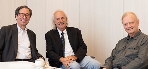
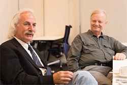
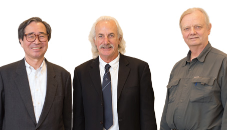
Three Pioneers of Nanoscience and Technology Got Together at MANA
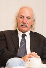
Don Eigler (Director, The Wetnose Institute for Advanced Pelagic Studies) and Stan Williams (HP Senior Fellow) were interviewed by Masa Aono (MANA Center Director)
Aono: Don and Stan, welcome to our research center MANA. I am really happy to have this opportunity to talk with you both here at MANA. In the past quarter century, I really enjoyed the competition and collaboration with you both in my research of nanoscience and technology. I would like to take this occasion to say thank you very much for that.
Today, as the Director of MANA, I will play the role of an interviewer of you both.
Today, as the Director of MANA, I will play the role of an interviewer of you both.
Aono: I feel you two are an interesting combination, with Don into basic research and Stan interested in applications as well.
Eigler: When you work for a company, the first rule is the financial success of your corporation. In IBM, nobody did basic research only because they were interested in it; all research had to be strategic research. In that sense, there is no difference between Stan's experience at Hewlett-Packard (HP) and my experience at IBM. My work at IBM was aimed at laying a foundation of knowledge that IBM could identify as being strategic to the company’s success in the future.
Aono: Your work on xenon manipulation on a nickel surface was really a breakthrough in nanoscience and technology.
Eigler: I did not intend to do that at the beginning. My goals were to develop a better understanding of how atoms bond with one another and with the surface. When we were carefully operating the low-temperature tunneling microscope, we were able to rearrange the atoms. Then, we attempted to get it under control.
Aono: Stan, you changed from being a surface scientist studying solid surfaces with ion scattering spectroscopy to studying devices such as the memristor. What was your motivation?
Williams: In 1994, the Northridge Earthquake completely destroyed my laboratory at UCLA. Simultaneously, I was offered an opportunity to start up a new fundamental science research group at HP. The concept was to build something from the foundation and create something unique and revolutionary for the company in 10 to 15 years. This would give HP an advantage in the future marketplace. Today, I run a group within HP called Foundational Technologies which focuses on the future, but my activities are concentrated toward bringing those technologies to the marketplace.
Aono: How did you encounter Leon Chua's idea?
[The memristor was predicted in 1971 by Leon Chua, an electrical engineer at the University of California, Berkeley.]
Williams: At HP, I spent some time looking at the technological landscape. At that time, Moore's Law had run its course. I started thinking what happens when Moore's Law stops and it is no longer possible to make smaller transistors. I intentionally looked at new types of electronic and photonic devices. I started looking at inorganic materials and working with atomic switches, and that was how I got into memristors. Concurrently, I was also looking at photonics and developed a photonic switch based on a ring resonator.
Aono: Don and Stan, I would like to hear your opinion about the future of nanoscience and technology.
Eigler: Nanoscale science has been going on for a long time. There are many opportunities for learning new things about the properties of materials and the strange behaviors that occur in nanostructures. I do not see nanotechnology having a big impact yet, but 15 to 20 years from now, the impact of controlling things on a nanometer length scale will change the way people do things. However, I do not know if this is a revolution.
Williams: Nanotechnology has been incredibly important, but not for the reasons that most people think. Nanotechnology attracted intelligent young people to come into this field. This influx of intelligent and motivated young people has created an important body of work. Now what we have is a foundation, and it is time to start building on top of that foundation.
Aono: Don, what do you think about the importance of interdisciplinary collaboration?
Eigler: I do not necessarily like the word interdisciplinary because it implies that there are necessary boundaries between the different sciences. One ramification of nanoscience efforts over the last 15-20 years is that many young people are being trained to think, work and communicate across a broad spectrum of the sciences. I regard that ability to combine knowledge and experience from separate fields as being hugely powerful.
Aono: Stan, what do you think about the importance of government science and technology policy?
Williams: Most people in government have got a wrong impression about what research is. Creation of new knowledge from academic research is an important byproduct, but the real product is the creation of highly skilled and motivated people who will be making new advances to keep a nation’s economy strong. Today, there is too much emphasis on what academic researchers are doing. I am trying to pound those ideas into people in the government, but sadly, we are seeing a situation where decision-makers are ignorant of the system for which they are making the decisions.
Aono: What do you think about the recent young scientists?
Eigler: The most rewarding aspect of my professional life has been being able to create opportunities for young scientists and then to see them grab on to those opportunities. Creating opportunities for young people is an obligation that a scientist has to shoulder to some extent; otherwise, science is going to die. Other human endeavors make our lives wealthier, but new fundamental knowledge drives humanity forward, and this comes through research.
Aono: Don, you could have hired many young scientists, but you have had a small group. Stan, your group is large and you are managing many young scientists very well.
Eigler: I wanted to be a part of a small group so that I could always be close to the science and hopefully get into a laboratory as much as I could. Even then, I was not very successful at that and I have spent less and less time in the laboratory.
Williams: I was brought into HP to create a new culture and introduce more foundational research. I was expected to build up that capability within the company, and it was clear that I would have a large group. However, I never expected it to get as large as it did. After the nanotechnology explosion in the 2000s, I kept finding very interesting young people and found creative ways to hire them. These people then went out and found new people.
Aono: What are your future plans in your research and life?
Eigler: I left IBM 3 years ago because I wanted to do something new. I have been thinking about fundamental physics experiments. For instance, I have spent time on how to do laboratory-scale measurement of the speed of gravity. Part of the reason I choose these things is because they are incredibly difficult, although not impossible.
Williams: I am thinking about cognition as an engineering exercise. My study concludes that people do not understand as much as they think they do about brain function, so I am trying to understand it in more mathematical detail. I am hoping that I can make a much bigger contribution to this understanding with the idea of trying to build an artificial brain. We are still probably centuries away from being able to build something as truly sophisticated as a real brain, but there are computational things that brains can do very efficiently that could make today's computers much more efficient.
Aono: Before this interview, both of you toured our labs at MANA. What is your opinion about MANA and your advice on the future of MANA?
Eigler: Jealousy! I am overwhelmed by the amount of resources that is available in MANA. I see MANA as being an investment that the Japanese people are making in their own future and also in the future of everybody else. Nothing even remotely close to MANA is happening anywhere else in the world.
Williams: I agree with Don. The work that is going on here is at the very top of anything in its class that is being done anywhere. It is a place where people can dream and can aspire to do things that others think are impossible. They have a chance to completely redefine the frontiers of understanding.
Aono: Oh, your words, the words from two pioneers in nanoscience and technology, will be a strong encouragement to all the scientists in MANA. I want to say a very sincere thank you to you both.
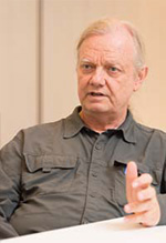
Don Eigler
Director, The wetnose Institute for Advanced Pelagic Studies
Dr. Donald M. Eigler is a physicist who has specialized in the development and use of low temperature scanning tunneling microscopes. His research is aimed at understanding the physics of nanometer-scale structures and exploring the applications of nanometer-scale structures to computing. He is best known for his 1989 demonstration of the ability to manipulate individual atoms with a low-temperature scanning tunneling micro-scope, famously spelling out the letters "IBM" with 35 xenon atoms. He received both his bachelors and doctorate degrees from the University of California, San Diego. He joined IBM as a Research Staff Member in 1986, was named an IBM Fellow in 1993 and left IBM in 2011 to become the director of The Wetnose Institute for Advanced Pelagic Studies.
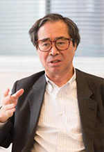
Stan Williams
HP Senior Fellow
Dr. R. Stanley Williams, one of the world’s leading scientists in nanotechnology, is a Hewlett-Packard Company (HP) Senior Fellow and the Vice President of Foundational Technologies at Hewlett-Packard Laboratories in Palo Alto, California. He received a B.A. degree in Chemical Physics in 1974 from Rice University and his Ph.D. in Physical Chemistry from the University of California, Berkeley in 1978. At HP, he led a group that developed a working solid state version of Leon Chua's memristor. His present research interests are nano-electronics and -photonics, computation and cognition. He has published over 400 original research papers in peer-reviewed journals and has been awarded over 300 patents worldwide.
Masa Aono
MANA Center Director
Dr. Masakazu Aono is currently the Center Director of MANA and also a NIMS Fellow. After receiving his Ph.D. from the University of Tokyo in 1972, he joined the National Institute for Research in Inorganic Materials (NIRIM) as a Research Staff Member. From 1978 to 80, he worked at the Synchrotron Radiation Center of the University of Wisconsin-Madison, USA, as a Visiting Professor with an IBM group headed by Dr. Dean Eastman. In 1986, he moved to the Institute of Physical and Chemical Research (RIKEN) as a Chief Scientist and organized the Surface and Interface Laboratory. From 1996 to 2005, he was concurrently a Professor of Osaka University. In 2002, he moved to NIMS as the Director of the Nanomaterials Institute and was then appointed to his present position in 2007. He has done various pioneering work in surface science, nanoscience, nanoelectronics and nanoscale measurement, symbolized by the words “impact-collision ion scattering,” “atomcraft,” “atomic switch,” “multiple-probe SPM” and “chemical soldering.”