1.1 Control of local ion migration and electrochemical reaction in a solid
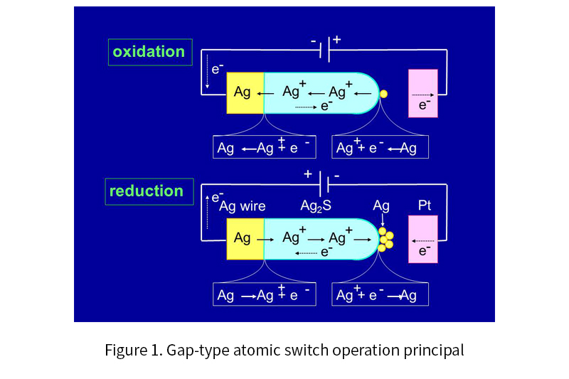
A silver sulfide (Ag2S) mixed conductor, capable of moving silver ions and electrons, is used as the probe for scanning tunneling microscopy (STM). By controlling the polarity and magnitude of the voltage applied between the Ag2S probe and the platinum substrate and the magnitude of the tunnel current, a nanometer-scale protrusion made of Ag atoms grows and shrinks at the tip of the Ag2S probe (Fig. 1). The growth and shrinkage of the Ag protrusion are caused by electrochemical phenomena in the Ag2S solid. Since the distance of the vacuum gap between the Ag2S probe and the platinum substrate is about 1 nm, when a negative voltage is applied to the substrate, tunnel electrons flow from the substrate toward the Ag2S probe, and Ag ions in the tip of the Ag2S probe become neutral Ag atoms due to the reduction reaction (Ag+(Ag2S) + e – → Ag) with tunnel electrons. Because neutral Ag atoms are unstable inside Ag2S, they precipitate on the surface of the Ag2S probe to form the Ag protrusion (Fig. 1 (a)). When the polarity of the voltage applied to the substrate is reversed to positive, tunnel electrons flow from the Ag protrusion at the tip of the Ag2S probe toward the substrate. In this case, the Ag atoms of the protrusion partially re-solidify/dissolve into the Ag2S probe by the oxidation reaction (Ag+(Ag 2 S) + e - ← Ag), and the Ag protrusion shrinks and disappears (Fig. 1 (b)). We found that an ON/OFF switch on the atomic scale can be created by exploiting the growth and shrinkage of the Ag protrusion.
1.2 Creation of the gap-type atomic switch
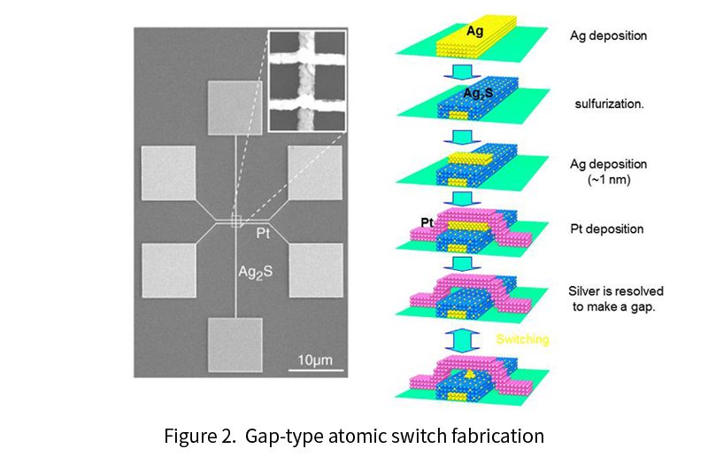
Based on fundamental study on the control of local ion migration and electrochemical reactions using tunnel electrons by STM, we have succeeded in creating an atomic-scale switch device (the gap-type atomic switch) that operates by locally moving several to several tens of atoms. The atomic switch is fabricated by utilizing conventional semiconductor fine-fabrication technology. A scanning electron micrograph and schematic diagram of the fabricated atomic switch are shown (Fig. 2 (a) (b)). The switch consists of a crossbar structure, formed by stacking Ag thin wire (electrode) / Ag2S thin wire / Ag thin film / Pt thin wire (electrode). The Ag thin film has a thickness of about 1 nm. Here, when a positive polarity voltage is applied to the Pt electrode, the Ag atoms constituting the Ag thin film become Ag ions due to an oxidation reaction and are dissolved into the Ag2S, whereby the Ag thin film disappears and a gap is formed between the Pt electrode and the Ag2S thin wire. In this state, tunnel electrons flow through this approximately 1 nm gap due to voltage application between the electrodes, but the electrical resistance shows a comparatively large value of several to several tens MΩ. Next, when a negative polarity voltage is applied to the Pt electrode, tunnel electrons flow from the Pt electrode to the Ag2S thin wire. When the voltage and tunnel currents are higher than a certain threshold value, the precipitation and growth of an Ag protrusion occurs on the Ag2S surface by the reduction reaction of the Ag2S wire Ag ions. Furthermore, the Ag cross-bridge is formed within the gap between the Pt electrode and the Ag2S thin wire, and the electric resistance remarkably decreases to several kilos to several tens of ohms (Fig. 2 (b)). Thereafter, when the polarity of the voltage applied to the Pt electrode is reversed positively, the Ag atoms constituting the cross-bridge become Ag ions by an oxidation reaction and re-solidify/solubilize in the Ag2S, thereby cutting/disappearing. Thus, ON / OFF operation of a gap-type atomic switch can be obtained on an atomic scale.
1.3 Emergence of various unique functions
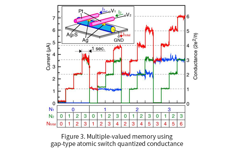
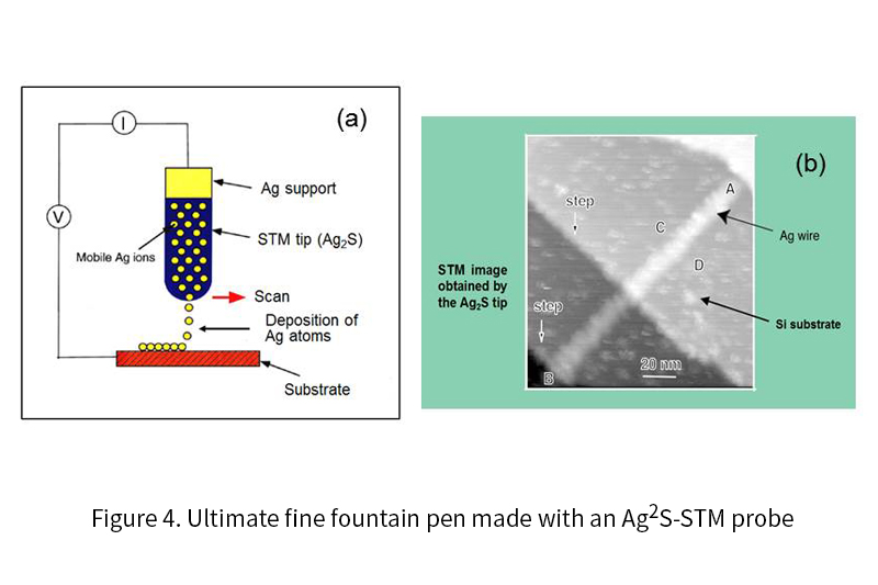
The gap-type atomic switch not only has a simple switch function but also has interesting functions and is useful for applications such as quantized conduction and multi-valued memory, logic gates for computation, nano-fountain pens, artificial synapses, decision making devices, and so on. For example, quantized conduction is found by precisely controlling the electrochemical reaction using positive and negative pulse voltage. In an atomic switch that has an Ag electrode / Ag2S / gap / Pt electrode structure, when a small pulse voltage is applied between the Pt electrode and the Ag electrode, the Ag protrusion slowly grows toward the Pt electrode and a point contact is formed between the Ag protrusion and Pt electrodes. This point contact emerges as quantized conduction because it can be controlled on the atomic scale. It is possible to create a multivalued memory by using this phenomenon. A 1 × 2 array consisting of a cross-bar structure of Ag electrode / Ag2S / gap / Pt electrode is fabricated, in which atomic switches are formed at two cross points. Each atomic switch exhibits quantized conduction by precisely controlling the applied positive and negative pulse voltages. The quantum state number can be arbitrarily switched accordingly by applying a voltage of appropriate polarity and magnitude in a pulsed manner. Figure 3 shows that 4 × 4 = 16 states can be obtained by connecting two atomic switches capable of producing four kinds of quantum state number, from 0 to 3. Multi-valued memory can be developed by using this function. In addition, as shown in Fig. 4 (a), a nano fountain pen can be formed by using the Ag2S crystal as the probe material of an STM and by applying an appropriate voltage between the probe and the substrate. The nano-pen can fabricate a metal thin wire by the continuous deposition of Ag atoms from the Ag2S probe. This probe is an ultimately small fountain pen using ink consisting of Ag ions in Ag2S. Using this nano pen, it is possible to draw Ag atom lines on a substrate. (Fig.4 (b))
2.1 Oxide-based atomic switch
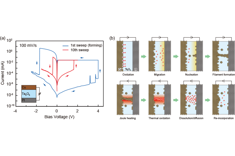
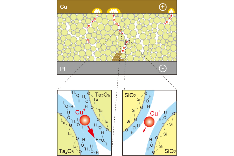
We have investigated the resistive switching mechanism and unique properties of a metal/insulator/metal (MIM)-structured atomic switches using Ta2O5 as the model matrix. Figure 1 shows the typical I-V characteristics and the corresponding operating mechanism of a Cu/Ta2O5/Pt cell. The cell is SET from the OFF state to the ON state under positive bias relative to the Cu electrode, and is RESET from the ON state to the OFF state under negative bias, indicating bipolar resistive switching behavior, as shown in Fig. 1(a). The SET operation consists of the anodic oxidation of Cu under bias applications, migration of oxidized Cu ions in the Ta2O5 matrix, and nucleation of Cu on the Pt electrode, followed by formation of a metal filament between the two electrodes. The RESET operation is attributed to thermal oxidation of Cu in the filament due to Joule heating and diffusion of Cu ions under ion concentration gradient and an electric field, as illustrated in Fig. 1(b). Repeated redox reactions at Cu(Ag)/Ta2O5 interfaces were observed by Cyclic Voltammetry, and the concentration and diffusion coefficient of the created ions were evaluated. Furthermore, we found that the morphology and deliquescency of Ta2O5 films affects the resistive switching characteristics of the oxide-based atomic switch, as illustrated in Fig. 2.
2.2 Polymer-based atomic switch
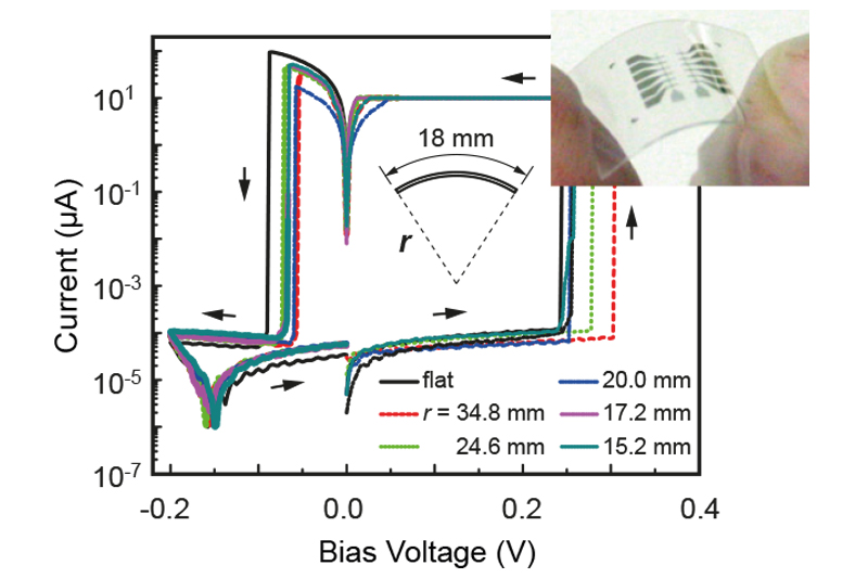
We have demonstrated that atomic switch operation can be realized with organic solid electrolytes. In a MIM structure using a solid polymer electrolyte (SEM), in which several percent of AgCIO4 is dissolved into Polyethylene oxide (PEO), resistive switching arising from the formation and dissolution of a metal filament was observed, similar to oxide-based atomic switches. PEO is well known as a Lithium-ion battery base material. Moreover, utilizing the mechanical flexibility of PEO, we succeeded in fabricating an atomic switch cell on a plastic substrate using an SPE film coated by ink-jet printing, and found that the cell exhibited stable switching characteristics under substrate bending, as shown in Fig. 3. This result indicates that the polymer-based atomic switch has potential for use in flexible electronics applications.
2.3 Conductance quantization and synaptic behavior
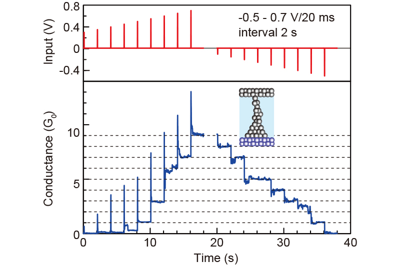
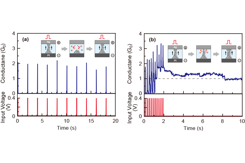
The unique properties of atomic switches are quantized conductance and synaptic behavior. We have succeeded in observing these characteristic behaviors in Ag/Ta2O5/Pt and Ag/PEO/Pt atomic switches. Figure 4 shows the conductance response when positive voltage pulses (0.3 – 0.7V, 20 ms width) are applied successively to an Ag/Ta2O5/Pt cell. By controlling the duration and amplitude of the voltage pulses, it is possible to increase the cell conductance in a stepwise manner. After that, if negative voltage pulses are applied, the cell conductance decreases in a stepwise manner and returns to the original OFF state. This behavior can be observed repeatedly. Similar behaviors are found in an Ag/PEO/Pt cell under voltage sweeping, in which the distribution of conductance states varies by changing the amplitude of the sweep voltage.
Cell conductance changes significantly when the interval times of the input voltage pulses are varied. Figure 5 represents the variation in cell conductance when voltage pulses are applied with different interval times. For long interval times, the cell conductance returns to zero immediately after the input pulses. In contrast, if voltage pulses are applied with short interval times, the cell conductance gradually increases with accompanying temporary increases and reaches integer multiples of G0 (conductance of a single atomic point contact). These conductance states are maintained for a certain time after the final pulse. This conductance behavior is analogous to the long-term potentiation of biological synapses, in which the strength of the synaptic weight (or conductance) depends upon the time interval between stimulating pulses. In order to achieve this synaptic behavior, at least ten transistors and software preprogramming are required. Since the atomic switch can emulate this function with a single cell, without any software programming, it has the potential for use as a building block for the next generation of neural network systems.
2.4 Three-terminal atomic switch
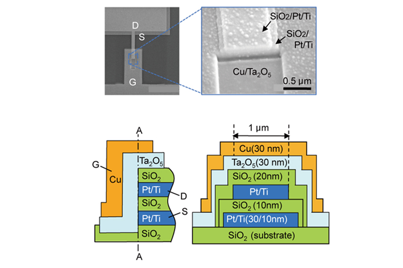
If the Pt electrode is divided by a thin insulating layer in a two-terminal structure and nucleation of metal atoms between the divided electrodes (source and drain) are controlled, it is possible to realize transistor operation in a three-terminal structure. We have achieved this three-terminal operation based on the movement of metal ions from a gate electrode. An SEM image and schematic illustration of the fabricated transistor are shown in Fig. 6. The Ta2O5 and gate layers are formed on the sidewall of the stacked source/SiO2/drain structure, which is prepared by focused ion beam etching.
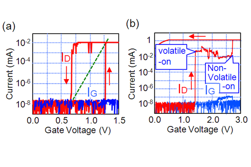
Figure 7 shows the typical operation of a three-terminal cell with a Cu gate electrode. As a positive bias voltage is applied to the gate electrode, the current between the source and the drain (drain current) increases by more than six orders to around 1.3 V. This drain current drops to a pA level of around 0.65 V if the gate voltage is swept back to 0 V from 1.5 V, indicating volatile behavior. On the other hand, when the gate voltage is swept to 3 V, another step of the drain current increase is observed around 2. 7 V. Once this current increase takes place, the resistance between the source and drain is kept low even if the gate voltage is swept back to 0 V, indicating nonvolatile behavior. Therefore, dual volatile/nonvolatile operations can be realized by controlling the gate voltage. The observed ON state is considered to originate from the formation and dissolution of a Cu nucleus between the source and drain electrodes, and the volatile and nonvolatile operations are determined by the structural stability of the Cu nucleus.
3.1 DECISION-MAKING FUNCTION MATHEMATICAL MODELS
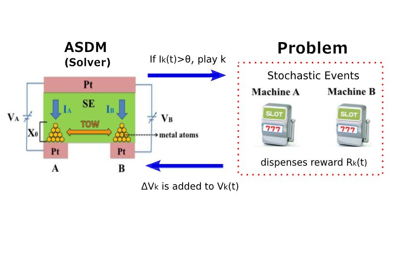
Slime mold ameba appears to able to minimize light stimulation by efficiently stretching either of its branches in a tug-of-war between the branches. From such behavior, we succeeded in extracting a novel computing principle of efficient decision-making called the "tug-of-war (TOW) principle." By applying the TOW principle to tug-of-war to the atomic masses precipitated in atomic switches, a decision-making device using atomic switches can be realized. We are implementing not only atomic switches but also ionic devices. It is possible to construct autonomous intelligent nanodevices that adjust their angles by themselves, like sunflowers, to maximize light absorption.
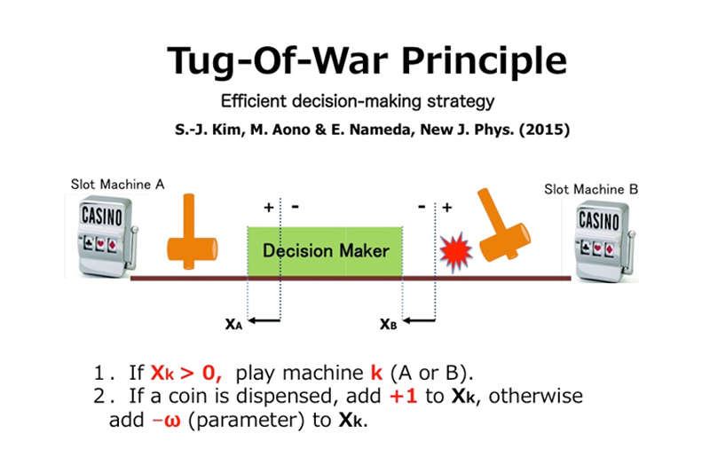
3.2 Tug-Of-War (TOW) Principle
TOW is a physical computing principle that solves the multi-arm bandit problem efficiently. As shown in Figure 1, the machine selected to play depends on the position of the object. It is supposed that in the state in which the object is shifted from the middle to the left side, machine A is selected, and machine B is selected on the right side. Here we assume that the object (center position) is always fluctuating. If a slot machine is played and a coin comes out, the object is moved by one unit in the forward direction (left in the case of A, right in the case of B). Otherwise, it is moved ω (Parameter) unit in the reverse direction (right in case of A, left in case of B). We have mathematically shown that coins can be acquired efficiently by repeating this process [1].
[1] S.-J.Kim, M. Aono, & E. Nameda, New J. Phys. 17, 083023, 2015.
3.3 The multi-armed bandit problem
For simplicity, consider four slot machines, as shown in Figure 2. It is assumed that each slot machine dispenses one coin at a predetermined reward probability (PA, PB, PC, PD). The player does not know these probabilities. Identifying the types of policies that will be able to maximize earnings reward is called multi-arm bandit problem. In essence, since the number of coins is variable and the reward probability (distribution) changes with time, the multi-arm bandit problem is regarded as very difficult in computation theory.

4.1 DECISION-MAKING DEVICES
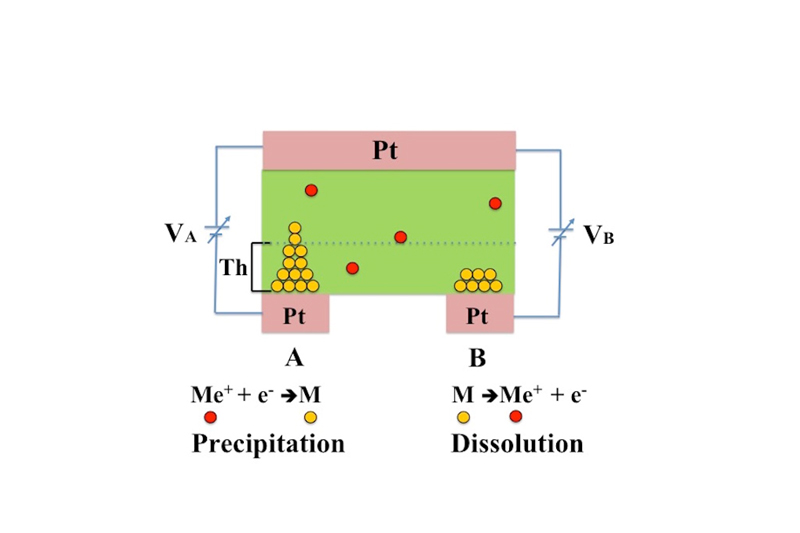
Research detailsFigure 1 illustrates an ionic decision-maker capable of operating using electrochemical phenomena induced by the movement of protons (H+) within a solid electrolyte. When the device makes a correct decision, ions migrate toward the electrode associated with the decision. Repeated correct decisions cause a variation in ionic/molecular concentrations and reinforce the decision. The device can solve multi-armed bandit problems (see 3.1) on the basis of tug-of-war principle. We applied this mechanism to a congested radio communication network and succeeded in demonstrating that the device is capable of selecting an optimum communication channel (i.e., frequency range) to be assigned for a given transmission in order to achieve the most effective overall channel utilization in relation to changing congestion situations (Figure 2). The device also demonstrated the capability to make optimum channel selections to meet an even more complex goal, i.e., achieving the most effective overall channel utilization among multiple communication network users (Figure 3 & 4).
Fig. 1: Schematic diagram of an ionic decision-maker capable of learning and decision-making using electrochemical phenomena.
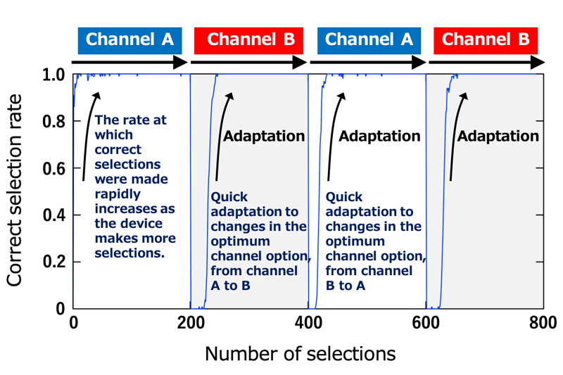
Fig. 2: The ionic decision-maker learns the current usage of communication channels A and B and quickly determines which should be assigned for a given transmission in order to achieve the most effective utilization of these channels. The diagram indicates optimum selections between channel A and B in relation to time.
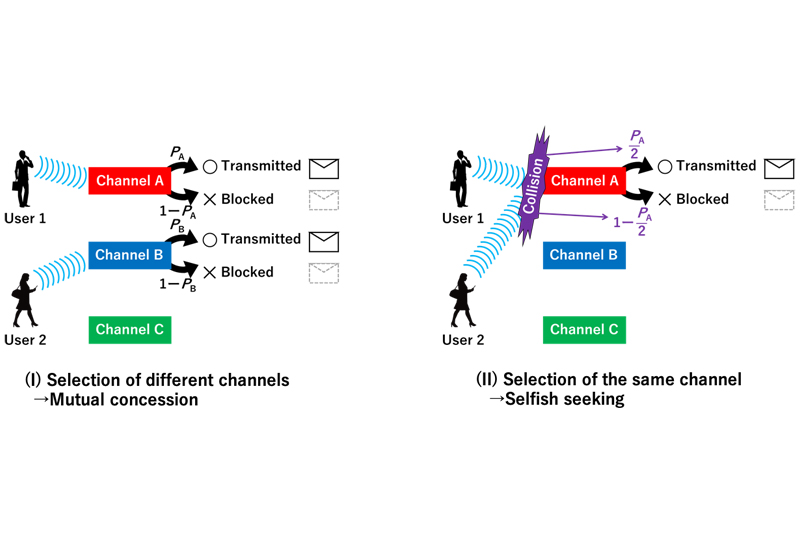
Fig. 3: Examples of two situations in which two network users are attempting to use different channels or the same channel in the network.
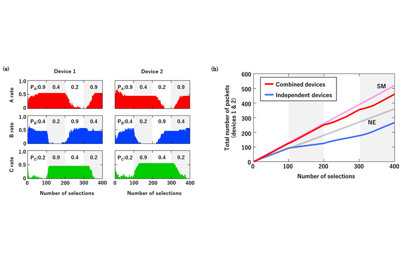
Fig. 4: (a) Variation in selection rates for channels for two devices. (b) Variation in total number of packets for devices 1 and 2 in two operation modes (combined devices and independent devices). SM and NE show theoretical limits of SM (pink dotted curve) and NE (gray dotted curve).
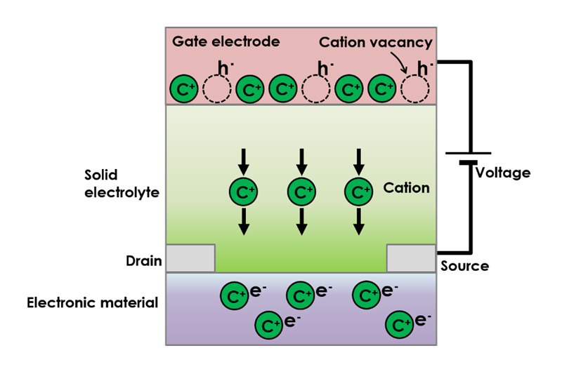
5.1 All-solid-state electric double layer devices & all-solid-state redox devices
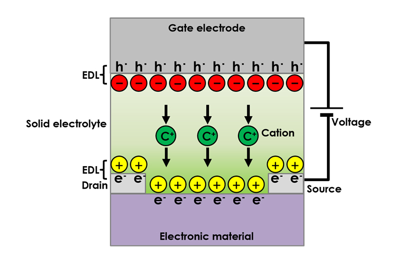
In the all-solid-state electric double layer transistor, illustrated in Figure 1., ion transport occurs inside a solid electrolyte layer, accompanied by the piling up of ions near the solid electrolyte/electronic material interface. An electronic carrier, with an opposite charge polarity, is accumulated in the vicinity of the interface due to charge compensation. That is to say, the electric double layer consists of high density ions and electronic carriers that face each other. The electronic carrier density can be reversibly controlled by the electric double layer because the charge density of the electric double layer depends on an external electric field (gate voltage). A significant advantage of the electric double layer is its huge capacitance (> several tenths µF/cm2), which leads to high density carrier doping despite the fact that the electric double layer transistor is an electrostatic carrier doping method, which usually exhibits small capacitance. The technique is particularly advantageous for application to electronic materials in which the physical properties of the electronic structures are sensitive to disturbance caused by chemical doping or nonstoichiometry (e.g. superconductivity).
Figure 2 illustrates the all-solid-state redox transistor. With this device, while ion transport occurs as in the electric double layer transistor, ions are also inserted in an electronic material. The electronic carrier is doped in the electronic material by charge compensation. The technique used for electronic carrier control is a redox transistor. Compared to conventional semiconductor technology, the advantage of this technique is that nonvolatile operation can be achieved with a redox mechanism, including relatively slow process times.
5.2 Pursuing high temperature superconductivity with all-solid-state electric double layer transistors
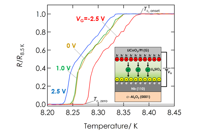
Superconductivity is a promising solution for solving energy and environmental problems, and is also important for the development of superconducting computers with extremely high performance and low power consumption. High temperature superconductivity, in particular room-temperature superconductivity, is the ultimate goal in solid physics. We are exploring high temperature superconductivity with high density electronic carrier doping in potential high temperature superconductors, using all-solid-state electric double layer transistors as the foundation. Figure 3 illustrates an all-solid-state electric double layer transistor, which is composed of lithium ion conducting solid electrolyte and niobium; a well-known metallic superconductor. The figure also shows the superconducting transition of niobium tuned by various gate voltage applications. High density electronic carrier doping in the vicinity of the interface enhances the superconducting temperature.
5.3 Bandgap tuning of graphene oxide achieved by redox reaction
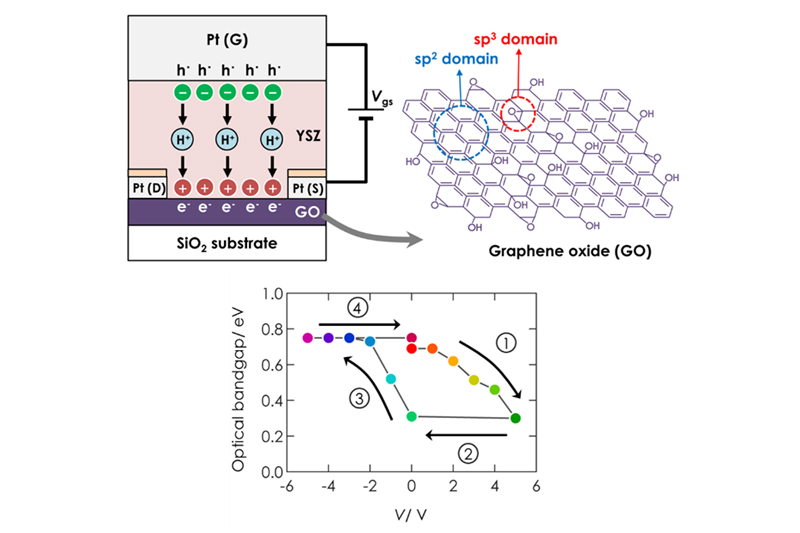
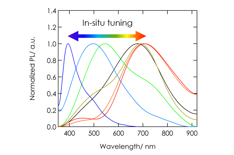
Graphene oxide (GO), a graphene sheet derivative modified with oxide functional groups, has attracted much attention as a material for exploring a variety of physical properties (e.g. electric properties, absorption, photoluminescence, and room-temperature ferromagnetism). The uniqueness of GO originates from electronic disorder due to sp3 hybridization carbon, which bonds mainly with oxygen atoms, in sp2 conjugated networks. The sp2/sp3 fraction positively correlates with the carbon/oxygen ratio (C/O), and dominantly affects the band gap width and other GO properties. We developed a multifunctional device that enables the in-situ tuning of various GO properties due to redox reactions. Figure 4 illustrates an all-solid-state redox and electric double layer transistor composed of multilayer GO and proton conducting solid electrolyte. The band gap was reversibly tuned by DC voltage application as shown in Figure 4. It is interesting that the device works as an electric-double-layer transistor with relatively small voltage. Figure 5 shows the photoluminescence of GO tuned by this technique. The reversible tuning is advantageous for application to ICT devices, optics, and biosensors.
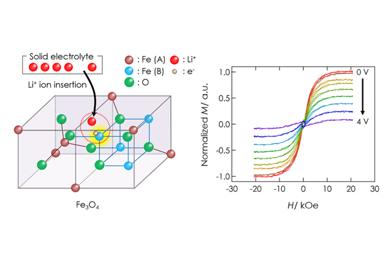
5.4 Magnetic property tuning for spintronics applications
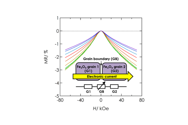
High-density magnetic storage devices (e.g. hard disks, magneto-optical disks, and MRAM) have become even more important due to the information explosion now underway. Since these devices operate on the basis of the tuning of magnetic properties, including magnetization, magnetoresistance (MR), and Kerr rotation angle, development of a technique for property tuning in thin film devices should lead to the generation of technological innovations in high-density storage, low power consumption, high operating speed, and so on. We have developed all-solid-state redox devices composed of ferromagnetic Fe3O4 thin film, which is a promising material due to its half metallicity. Figures 6 and 7 show magnetization and the MR effect tuned by DC voltage application. Magnetization and MR were reversibly tuned by modulation of the spin number in the Fe3O4 due to the insertion and removal of lithium ions.
6.1 Controlled chain polymerization
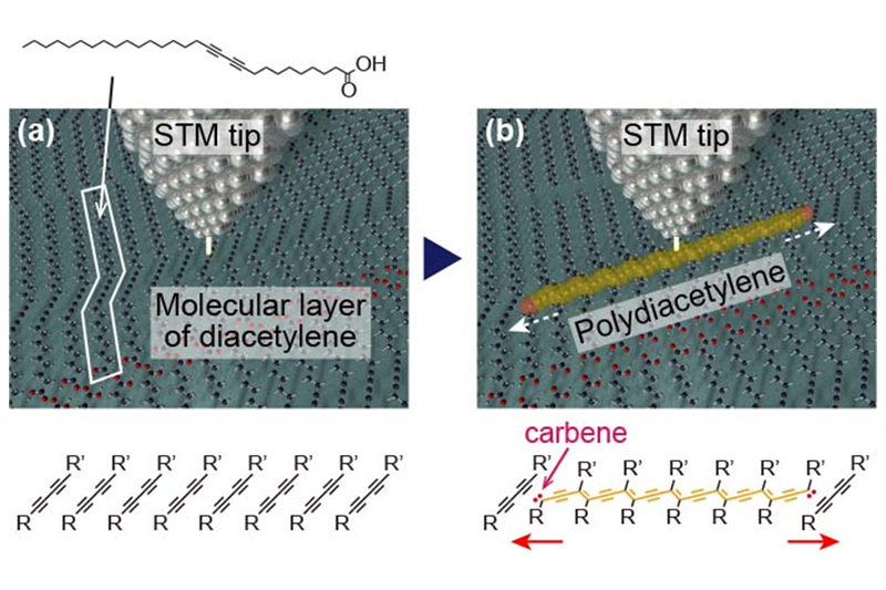
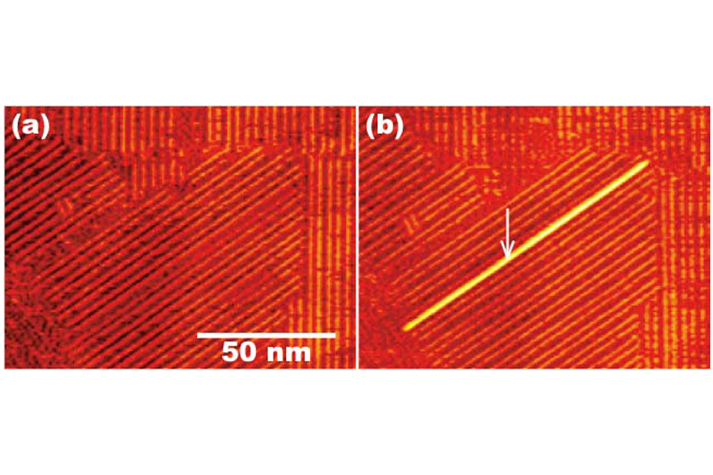
Development of a nanowiring technology for transmitting electricity at nanometer widths is indispensable for realizing molecular scale devices. The best way to reduce the width of wires to that of single molecules is to connect the nanodevices with conductive organic polymers. We have developed a method for controlling the chain polymerization of organic molecules with spatial resolution on the order of 1 nm, and succeeded in fabricating single conductive polymer nanowires at designated positions [1]. The procedure is illustrated in Figure 1. The organic molecule used is a diacetylene compound that contains two C≡C triple bonds. When placed on a graphite substrate by an appropriate method, these molecules spontaneously form a monomolecular film with the molecules arranged in a regular pattern of straight lines (self-assembled monolayer). Next, a pulse voltage is applied to one arbitrarily selected molecule using the probe tip of a scanning tunneling microscope (STM). This triggers a one-dimensional chain polymerization originating at that molecule, and forms a conductive polydiacetylene compound. As a result, by applying a single stimulus at one arbitrary point, a conductive one-molecule-wide polymer nanowire can be fabricated. Figure 2 shows STM images before and after the chain polymerization. The bright line in Figure 2(b) is the formed single polydiacetylene chain.
This technique offers numerous advantages. For example, the polydiacetylene chains obtained by this method are long and straight and without any defects. Moreover, the procedures can be conducted at room temperature, not only in vacuum but also at air/solid or liquid/solid interfaces.
1) “Nanoscale control of chain polymerization”, Y. Okawa, M. Aono, Nature 409 (2001) 683.
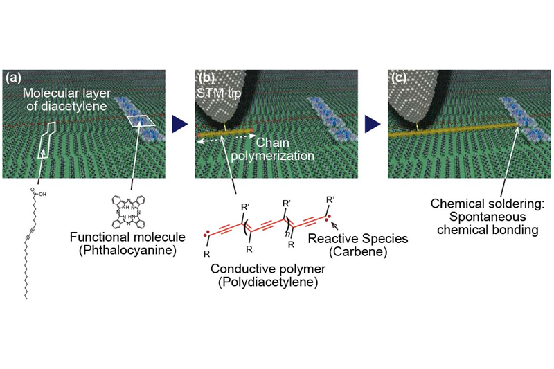
6.2 Chemical soldering
Single molecule electronics devices have been proposed as a promising candidate for next-generation nanodevices. In single molecule electronics, the individual molecules function as electronic components, such as rectifiers and switches. Although single-molecule electronics has been widely investigated over a long period of time, the fabrication of practical single-molecule circuits remains challenging because of the lack of viable methods for wiring each molecule. The method for connecting each functional molecule with single conductive polymers is thus a key technology for the development of single molecule electronics.
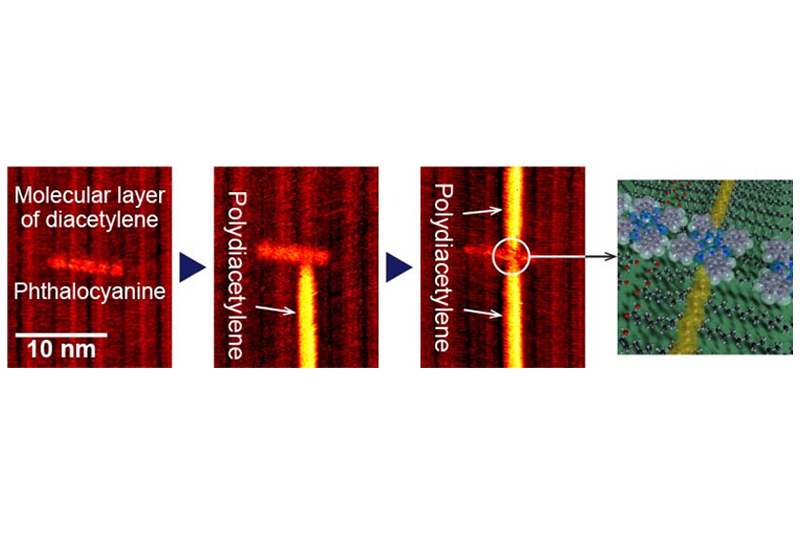
We have found a novel method for controlling on-surface single-molecule chemical reactions, which enables us to connect single conductive polymer chains to single organic molecules. We have named the method “chemical soldering” [2]. Figure 3 shows a schematic illustration of the wiring procedure. First, the relevant functional molecules are placed on a self-assembled monolayer of a diacetylene compound (Fig. 3(a)). The tip of a scanning tunneling microscope (STM) is then positioned on the molecular row to which the functional molecule is adsorbed, and a conductive PDA chain is fabricated by initiating chain polymerization as described before (Fig. 3(b)). Since the front edge of chain polymerization necessarily has a reactive chemical species, such as carbene, the created polymer chain spontaneously forms covalent bonding with an encountered molecular element (Fig. 3(c)).
The demonstrations were performed using phthalocyanine (Pc) as the functional molecule (Fig. 4). When a small amount of Pc was deposited on a self-assembled monolayer of diacetylene compound (10,12-nonacosadiynoic acid), we found that nanoclusters consisting of five Pc molecules stabilized on the layer. Two PDA chains were then connected to a single Pc molecule using the chemical soldering method. The estimated electronic states predict that the fabricated polydiacetylene–Pc–polydiacetylene system will act as a resonant tunneling diode.
2) “Chemical wiring and soldering toward all-molecule electronic circuitry”, Y. Okawa, S. K. Mandal, C. Hu, Y. Tateyama, S. Goedecker, S. Tsukamoto, T. Hasegawa, J. K. Gimzewski, M. Aono, J. Am. Chem. Soc. 133 (2011) 8227.
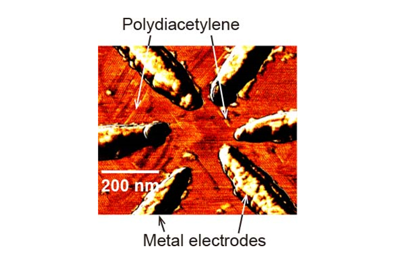
6.3 Development of methods to measure the functions
It is not possible to use a conductive substrate, such as graphite, to measure the electrical transport properties of the single conductive polymer chains or single molecule devices described above, and thus have to fabricate the devices on an insulating substrate. So we searched for an atomically flat insulating substrate on which diacetylene compounds could form flat-lying self-assembled monolayers for chain polymerization, and found that hexagonal boron nitride (h-BN) was a good substrate for this purpose. We fabricated metallic nano-electrodes on an h-BN substrate, onto which we deposited diacetylene compounds. Figure 5 shows that single polydiacetylene chains are formed between the nano-electrodes [3]. In addition to this method, we are investigating a method to measure the electrical transport properties using a functionalized graphene substrate. These studies will be an important step forward in demonstrating the functions of single-molecule electronic devices.
3) “Self-assembled diacetylene molecular wire polymerization on an insulating hexagonal boron nitride (0001) surface”, M. V. Makarova, Y. Okawa, E. Verveniotis, K. Watanabe, T. Taniguchi, C. Joachim, M. Aono, Nanotechnology 27 (2016) 395303.
7.1 Fabrication of wide-bandgap oxide nanowire devices
In the fabrication of gas sensors using oxide wires, the surfaces of the oxide wires need to be clean, without surface contamination by chemical reagents like resist. For the end, we have developed new techniques to make sensors using probe-manipulation of oxide wires [1]. This enables wires to be moved onto pre-patterned electrodes without chemical surface contamination (Highlights 2009 in Nanotechnology).
[1] M Sakurai, Y G Wang, T Uemura and M Aono “Electrical properties of individual ZnO nanowires”, Nanotechnology 20, (2009) 155203-1.
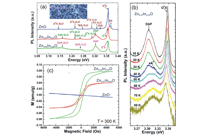
7.2 In-doped ZnO nanowires
Impurity doping usually reduces the crystal quality of oxide materials and induces large changes in their properties. We fabricated In-doped ZnO nanowires and studied the changes in their properties as a function of dopant concentration. We found a new DAP mode, caused by donor-acceptor parings in their PL spectra at low temperature, and observed room-temperature ferromagnetism for the In-doped ZnO nanowires.
[2] K. W. Liu, M. Sakurai and M. Aono : “Indium-doped ZnO nanowires: Optical properties and room-temperature ferromagnetism” J. Appl. Phys. 108, (2010) 043516-1
7.3 Au nanoparticle-decorated ZnO nanowires
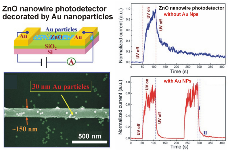
We found a large enhancement of the UV light-induced response in ZnO nanowires decorated by Au nanoparticles with a diameter of 30 nm. This novel property can be applied to high sensitivity UV-photo sensors.
[3] K. Liu, M. Sakurai, M. Liao and M. Aono : “Giant Improvement of the Performance of ZnO Nanowire Photodetectors by Au Nanoparticles” J. Phys. Chem. C 114, (2010) 19835.
[4] K. Liu, M. Sakurai and M. Aono : “ZnO-Based Ultraviolet Photodetectors” Sensors 210, (2010) 8604.
7.4 Wide-bandgap oxide core/shell microwires
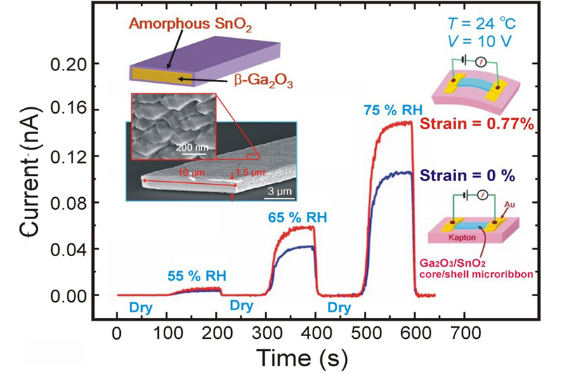
We fabricated core/shell microwires of two wide-bandgap materials with different melting points through vapor growth in an electric furnace. The Ga2O3-SnO2 core/shell microwires, formed from β-Ga2O3 microrods covered by thin amorphous SnO2 layers with a thickness of about 300 nm, have large surface area shells. With this core/shell structuring, the conventional adsorption of water on the SnO2 surface has been increased and high functional humidity & temperature sensors have been realized. Furthermore, bending the core/shell wires has increased their functions.
[5] K. Liu, M. Sakurai and M. Aono : “One-step fabrication of β-Ga2O3–amorphous-SnO2 core–shell microribbons and their thermally switchable humidity sensing properties” J. Mater. Chem., 22 (2012) 12882.
[6] K. Liu, M. Sakurai and M. Aono : “ Enhancing the Humidity Sensitivity of Ga2O3/SnO2 Core/Shell Microribbon by Applying Mechanical Strain and Its Application as a Flexible Strain Sensor ” Small 8, (2012) 3599.
7.5 Single-crystal SnO2 microwires
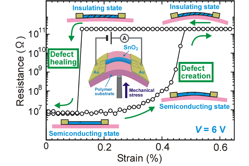
Rutile structured SnO2 does not have a piezoelectric effect due to its inverse symmetry. Utilizing this characteristic, we have demonstrated novel semiconductor-insulator transitions in SnO2 microwire devices. The reversible manipulation of lattice defects is possible due to defect creation by mechanical bending and defect healing by Joule healing. The reversibility originates from the formation of slipping planes in the rutile structure. The structures operate as ultra-sensitive UV-photo sensors by the combination of the characteristics of SnO2 and the sizing effect. We used the reversible manipulation of defects as a reset function for light-excited carriers in oxide materials, then we resolved the PPC problem; which is a well-known and serious problems in UV-photo detectors.
[7] K. Liu, M. Sakurai, M. Aono : “Controlling Semiconducting and Insulating States of SnO2 Reversibly By Stress and Voltage” ACS Nano 6, (2012) 7209.
[8] M. Sakurai, K. Liu, M. Aono : “Reversible and nonvolatile modulation of electrical resistance in SnO2 by external strain” Appl. Phys. Express 7, (2014) 031101-1.
[9] KW Liu, M. Sakurai, M. Aono, D. Shen : “Ultrahigh-Gain Single SnO2 Microrod Photoconductor on Flexible Substrate with Fast Recovery Speed” Adv. Funct. Mater. 25, (2015) 3157.