

I prepare the nitride semiconductor samples on the various substrates such as AlN templates /sapphire or SiC and GaN bulk substates by MOCVD. 2DEG carriers induced at the interface AlGaN/GaN and AlGaN/InGaN heterostructures exhibit Shubnikov de Haas (SdH) oscillation. The HEMT devices processed from these samples exhibited the good performance. Photothermal deflection spectroscopy (PDS) can detect the defect density as low as ~1014 cm-3 of order or less. The mechanism of in-gap emissions was discussed in the viewpoint of structural disorder or defect in the bandgap evaluated by PDS. Oxidation behaviors on various GaN surfaces were provided with the experimental data and molecular dynamics calculation.

Next-Generation Semiconductor Group
STAFF
Group leader
Group members
AIM and GOAL
Focusing on nitride and diamond semiconductors, we will promote the development of next-generation semiconductor materials and optoelectronic devices in an integrated manner, including heterojunction, epitaxial growth, microfabrication, and processing technologies, and establish guidelines for material device design and operating principles.
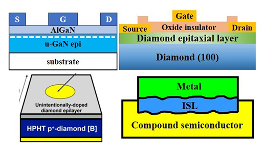
FIG 1 Schematic drawing of various optoelectronic devices aimed at in the next-generation semiconductor group
APPROACH
- Lead to improvement of the performance of high-electron mobility transistors and photoelectric conversion devices by improving the quality of nitride semiconductor thin films and advancing their functions based on an understanding of physical phenomena.
- Improve the reliability of nitride semiconductor devices by exploring the effects of environmental atmosphere and material properties on their characteristics.
- Improve the response characteristics of diamond deep-ultraviolet detectors to vacuum ultraviolet and proton beams and the long-term stable operation of the devices.
- Develop diamond logic circuits which are robust under extreme conditions by combining metal-oxide-semiconductor field-effect transistors with normally-on/off operation modes.
- Develop insulating gate materials and low-resistance ohmic contact materials for diamond and nitride semiconductors, and establish material design guidelines for semiconductor interfaces.
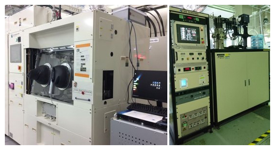
FIG 2 Photos of vapor phase growth equipment for nitride and diamond semiconductors.
SUMIYA, Masatomo
mail:SUMIYA.Masatomo@nims.go.jp
Development of novel functions from the formation of heterostructure composed of polar nitride semiconductors
Overview
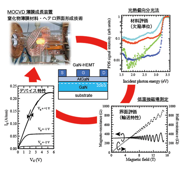
I have studied the mechanism of polar direction of nitride semiconductor film by metalorganic chemical vapor deposition. Unique electronic state is formed at the heterointerface of AlGaN/GaN by the polarity along c-axis (spontaneous polarization) and in-plane strain (piezo electric field). The defect levels in the bandgap are characterized by photothermal deflection spectroscopy The carrier transport of two-dimensional electron gas at the heterointerface is investigated under the high magnetic field at low temperature. Improving the nitride semiconductors and understanding the physical properties, novel functions will be developed from the formation of heterostructure composed of polar nitride semiconductors.
The achievements will be resulted in the high electron mobility transistors and photoelectric conversion devices.
Characteristics
Growing nitride semiconductor samples by metalorganic chemical vapor deposition, I have studied the basic physical properties such as defects in the bandgap, carrier transport at 2DEG, and surface oxidation for improving the device performance of LED, HEMT, and photovoltaic. The system of photothermal deflection spectroscopy has been developed originally for nitride semiconductor materials to detect the defect levels in the bandgap. 2DEG carrier transport has been analyzed together with a collaboration with the magnetic field group in NIMS. Theoretical GaN surface model taking the polarity into account was realized through the collaboration with RIKEN researcher.
Major reserch
Summary
- Nitride semiconductor materials of film and heterostructures grown by MOCVD
- Evaluation of defect levels in nitride semiconductors by PDS
- Characterization of 2DEG transport in high magnetic field at low temperature
- Theoretical and experimental approach to the surface oxidation on nitride semiconductor surface
- Improvement of performance composed of nitride semiconductors.
IROKAWA, Yoshihiro
mail:IROKAWA.Yoshihiro@nims.go.jp
Characterization of semiconductor devices
Overview
Reliability of semiconductor devices is a critical issue. For example, ambient atmosphere is known to alter the device characteristics, but the fundamental mechanism of the phenomenon is still unclear.
In this research, the effects of ambient atmosphere on nitride-based semiconductor devices are investigated.
Characteristics
Proposal of the physical model and development of hydrogen sensors
Major reserch
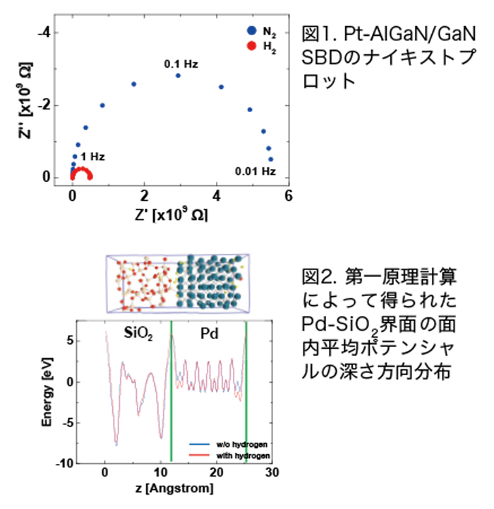
We investigated the metal/semiconductor interfaces. Figure 1 shows Nyquist plots of Pt-AlGaN/GaN SBDs. As shown in Fig. 1, a new semi-circle representing electric double layers are not confirmed. Figure 2 shows the calculated average potential at Pd-SiO2 interfaces. As shown in Fig. 2, the average potential at Pd-SiO2 interfaces does not changed after hydrogen introduction.
Based on these results, formally proposed hydrogen induced dipole model would not be the responsible mechanism. Through vigorous study, we have confirmed that dielectric layers at metal/semiconductor interfaces play a critical role.
Summary
Obtained results would be applicable not only to contributing to the reliability of semiconductor devices but also to the improvement of hydrogen sensors.
IMURA, Masataka
mail:IMURA.Masataka@nims.go.jp
Development of optical, electronic, and magnetic devices using next-generation semiconductors
Overview
In the field of next-generation semiconductor optical, electronic, and magnetic devices, the introduction of wide-gap semiconductors to replace Si is essential. I have focused early on III-nitride semiconductors and diamond semiconductors, which possess excellent applicability, practicality, and high potential, and am developing devices using these materials.
At NIMS, we have established a research system where crystal growth, device processing, and crystal evaluation are integrated, working together with constant feedback.
Characteristics
- Development of radiation and proton detectors using diamond semiconductors
- Development of full-spectrum visible light photonic devices using InGaN-based nitride semiconductor with nanofabrication
- Development of high-efficiency ultraviolet light-emitting diodes using AlGaN-based nitride semiconductors
- Development of high-frequency power devices using AlGaN/GaN and AlInN/GaN heterostructures
- Development of magnetic devices using BAlN and ScAlN-based nitride semiconductors
Major reserch
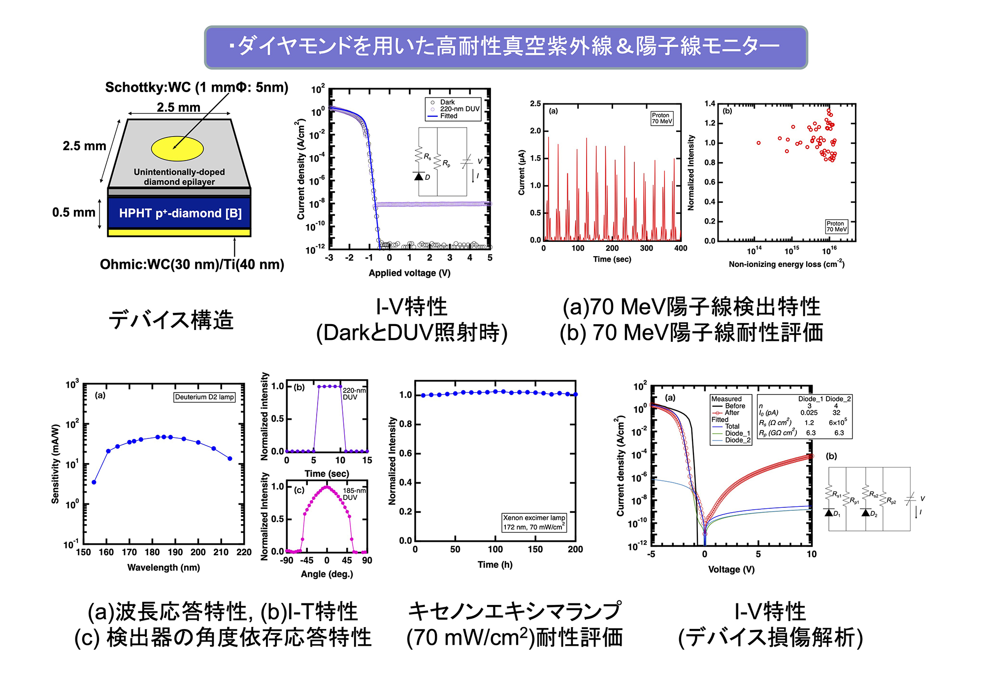
To realize a highly durable vacuum ultraviolet and proton detector capable of long-term stable operation with low power consumption, we fabricated a vertical Schottky barrier photodiode (SBPD) using diamond and evaluated its basic characteristics and durability.
Conductive diamond substrates were used to reduce charging effects. Low power operation was achieved by operating the device in zero-bias mode.
Furthermore, we evaluated the response characteristics and device durability against vacuum ultraviolet radiation and proton beams.
Summary
Using diamond, we fabricated detectors and evaluated their response characteristics and durability when exposed to vacuum ultraviolet radiation and proton beams. The results demonstrated the device's capability for long-term stable operation.
Recently, we have been conducting research and development on full-spectrum visible light photonic devices, high-efficiency ultraviolet light-emitting diodes, high-frequency power devices, and magnetic devices using novel materials, all based on Group III nitride semiconductors.
LIU, Jiangwei
mail:LIU.Jiangwei@nims.go.jp
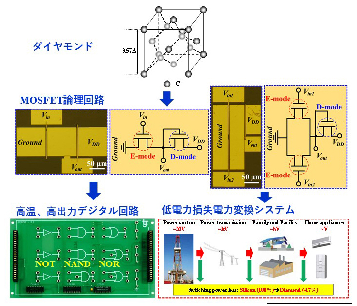
Diamond MOSFET Logic Circuits
Overview
Diamond is expected to be applied to power switches and integrated circuits that operate stably at high temperatures, high power, and high frequencies due to its high carrier mobility, large breakdown field, and high thermal conductivity.
As the first step towards developing diamond integrated circuits for extreme environments, we have successfully developed diamond logic circuits combining metal-oxide-semiconductor field-effect transistors (MOSFETs) with normally-on/off operation modes.
Characteristics
- Development of diamond MOS capacitors with extremely low leakage current density
- Development of control processing for normally-on/off operation of diamond MOSFETs
- Development of diamond MOSFET logic circuits
- Development of diamond power conversion systems with high thermal stability and low power loss
- Development of high-current output multi-gate diamond MOSFETs
Major reserch
In 2012, the interfacial band configurations of various oxides on hydrogen-terminated diamond (H-diamond) were determined using photoelectron spectroscopy technique. It was concluded that the large band offset energy at the Al2O3/H-diamond interface is advantageous for high-performance MOS electronic devices.
In 2013, the H-diamond MOS capacitors with extremely low leakage current density were achieved, along with the challenging development of normally-off H-diamond MOSFETs.
In 2014, NOT logic circuits were fabricated using H-diamond MOSFETs and load resistors. In 2015, control processing for fabricating normally-on/off H-diamond MOSFETs was achieved. In 2017 and 2018, the H-diamond logic circuits combining normally-on/off MOSFETs were fabricated successfully.
The diamond MOSFET logic circuits are promising for the application of high-temperature, high-power, low power-loss, and high thermal stability diamond digital circuits and power conversion systems.
Summary
Diamond logic circuits are expected to be applied to electronic devices that operate stably in extreme environmental conditions such as high-temperature, radiation, space, high-power, and high-frequency.
In order to push forward the development of diamond logic circuits for high current and high voltage applications, further improvement in mobility through higher-quality MOS interfaces and the introduction of voltage-resistant layers in the drain region will be necessary. We will continue to improve the electrical performance of diamond MOSFET logic circuits.
 Ultra-wide Bandgap Semiconductors Group
 Optical Single Crystals Group