What's Atom Probe Tomograpyhy (APT)?
 | NIMS提供APTデータセット | アトムプローブ装置群
 アトムプローブ法の概要:
3次元アトムプローブ(APT: atom probe tomography, or 3DAP; three-dimentional atom probe)は、曲率半径~ 50 nmの針状試料先端からイオン化された原子が検出器に到達するまでの飛行時間(Time-of-Flight)と検出位置(x, y)を連続的(z)に計測することにより、100万倍以上の倍率での原子分布を3次元に可視化できる唯一の手法です。原理としては、針状試料に高い電圧を印可することで試料先端に高電界を形成し、レーザーパルス(もしくは電圧パルス)照射をトリガーとして電界蒸発(イオン化)を誘発させます。アトムプローブを用いることでナノスケールのデバイスでの元素分布、材料内の元素の不均一な分布、半導体ドーパントなどの微量添加元素を精度良く解析することができます。
Atom probe tomography (APT, or 3DAP; three-dimentional atom probe) is the only method to visualize the distribution of atoms as 3D map at a magnification ratio of over 1 million by simultaneously measuring the mass and position of atoms ionized with laser pulses (or voltage pulses) from the needle-shaped specimens with the radius of curvature ~ 50 nm. For example, this method can precisely analyze the 3D distribution of elements within nanoscale devices or the uneven elemental distributions within materials.
Atom probe tomography (APT, or 3DAP; three-dimentional atom probe) is the only method to visualize the distribution of atoms as 3D map at a magnification ratio of over 1 million by simultaneously measuring the mass and position of atoms ionized with laser pulses (or voltage pulses) from the needle-shaped specimens with the radius of curvature ~ 50 nm. For example, this method can precisely analyze the 3D distribution of elements within nanoscale devices or the uneven elemental distributions within materials.
標準アトムプローブデータセット(NIMS提供):
アトムプローブ(APT)法による組織解析は主に(1) 針状APT試料の作製、(2) APT測定、(3) APTデータ解析の3つのステップに分けられます。近年では、商用APT装置のハードウェアおよび測定プログラムの劇的な進化によって、「(2) APT測定」は自動化が比較的進み、操作者にとってのハードルは下がってきました。その一方で、経験や技能が求められる「(1) 針状APT試料作製」と、APTの原理から材料に至るまで幅広く高い専門知識が必要な「(3) APTデータ解析」が、APT法の活用において障壁となっているのが現状です。そこで、ここでは「(3) APTデータ解析」の一助となるべく、典型的な材料のAPTデータセットを随時公開していく予定です。(※データセットはARIM Data Portalを通じて構造化され提供されます。)
| Structured APT Datasets | Model | DOI |
|---|---|---|
| 深紫外レーザーを用いたアトムプローブによる質量分解能の向上(ステンレス鋼) | Invizo6000 | 10.71947/arim.jpmxp1225nm2502-4 |
| 深紫外レーザーを用いたアトムプローブによる質量分解能の向上(コルソン合金) | Invizo6000 | 10.71947/arim.jpmxp1225nm2502-2 |
| Fe-B-P-Cuナノ結晶軟磁性材料のレーザーアトムプローブ分析における質量分解能の試料形状依存性 | LEAP5000XS | 10.71947/arim.jpmxp1225nm2502-6 |
| ステンレス鋼のレーザーアトムプローブ分析における質量分解能の試料形状依存性 | LEAP5000XS | 10.71947/arim.jpmxp1225nm2502-3 |
| コルソン合金のレーザーアトムプローブ分析における質量分解能の試料形状依存性 | LEAP5000XS | 10.71947/arim.jpmxp1225nm2502-1 |
| レーザー補助電界蒸発により安定的に分析可能となった銅系材料のアトムプローブデータ | LEAP5000XS | 10.71947/arim.jpmxp1225nm2502-5 |
アトムプローブ装置群:
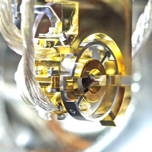
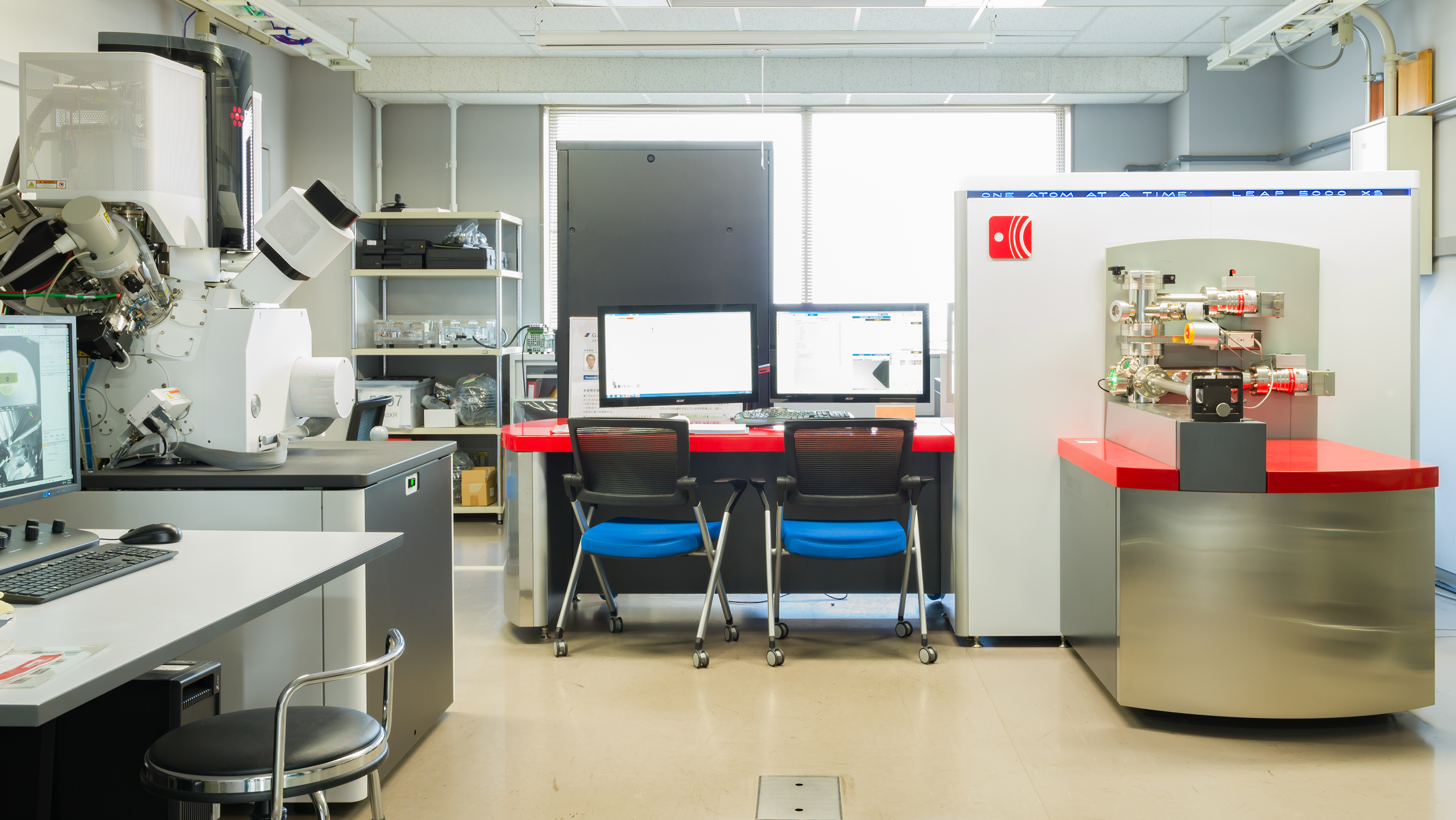
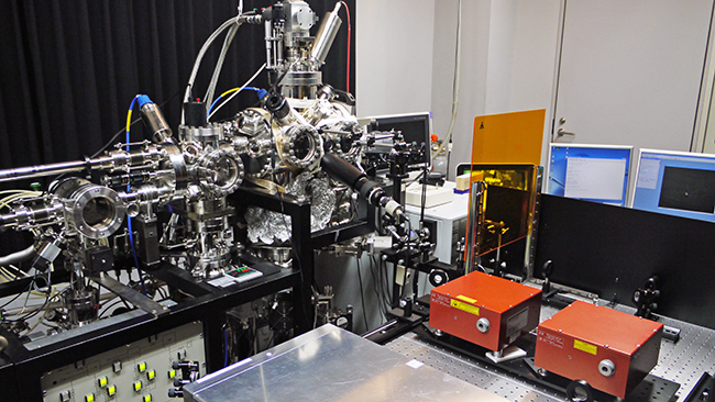
| 機種 | Invizo6000 (AMETEK) |
LEAP5000XS (AMETEK) |
NIMS-in-house developed Laser-assisted APT | LEAP6000XR (AMETEK) |
LEAP5000XR (AMETEK) |
|---|---|---|---|---|---|
| 外観 | 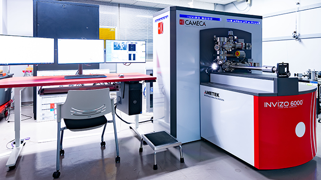 |
 |
 |
* Not at NIMS | * Not at NIMS |
| イオン軌道 | Straight | Straight | Straight | Reflectron | Reflectron |
| 検出効率 | ~ 62 % | ~ 80 % | 30 ~ 40 % | ~ 50 % | ~ 50 % |
| レーザー | 257.5 nm | 355 nm | 1030, 515, 343, 257.5 nm | 257.5 nm | 355 nm |
| 特長 | 新設計のイオン軌道による従来比較で4倍以上の分析視野/DUVレーザーによるデータ品質向上 | TEM/APT同一視野解析が可能/試料の大気非暴露&低温維持搬送が可能/検出効率 ~ 80% | レーザー波長可変式で、短波長化(UVレーザー採用)により世界で初めて絶縁体バルクのAPT解析に成功 | DUVレーザー+電圧パルスの同期による質量分解能追及 | 質量補正リフレクトロン採用による質量分解能重視型 |
| RMKS | 電子顕微鏡ユニット(内部共用: カテ2) | 磁性・スピントロニクス材料研究センター(内部共用: カテ3) | N/A | N/A | N/A |