Tutorials on 3DAP technique
* 2010年前後に執筆されたチュートリアルであることをご了承ください。執筆時以降、3次元アトムプローブ法は飛躍的に進歩していますが、手法の原理や歴史的背景を理解する上で重要であろうという意図から、当時のチュートリアルに部分的に加筆修正したのみで掲載しております。* Please note that this tutorials was written around 2010. Although 3D atom probe techniques have advanced dramatically since then, we are keeping posted this tutorials with only partial revisions to the original one. This may be essential for understanding the fundamental principles and historical background of the technique.
日本語版目次
- 電界放射顕微鏡(Field Emission Microscope; FEM)と電界イオン顕微鏡(Field Ion Microscope; FIM)

- 電界イオン顕微鏡(FIM)とは?
- FIM像解釈の基礎
- 電界蒸発(Field Evaporation)とアトムプローブ
- アトムプローブ電界イオン顕微鏡
- 3次元アトムプローブ(3DAP)の原理
- レーザーアトムプローブ
Table of Contents in English
- Principle of Field Ion Microscope (FIM)
- Field Evaporation & Atom Probe
- Atom Probe Field Ion Microscope (APFIM)
- Principle of Three-Dimensional Atom Probe (3DAP)
- Laser-assisted 3D Atom Probe (3DAP)
電界放射顕微鏡(FEM)と電界イオン顕微鏡(FIM)
電界放射顕微鏡(Field Emission Microscope; FEM)と電界イオン顕微鏡(Field Ion Microscope; FIM)はいずれも、先端を鋭く尖らせた金属の針状試料に高電圧を印加することにより試料表面で生ずる極めて高い電界による現象を利用した投影型顕微鏡である。装置は図1に示されるように超高真空チェンバーと針状試料を冷却するための極低温冷凍機、像を結像するための蛍光板から構成されている。FEMとして使用する場合は試料に負の高電圧を印加し、FIMとして使用するときには真空中に結像ガスを導入し試料に正の電圧を印加する。先端の半径がrの針状試料に電圧Vを印加したときの試料表面での電界FはF = V/rkであたえられる。ここでkは試料の形状による定数であり、通常5 ~ 7程度の値である。FEMでは電界放射に必要な電界強度が109 V/m程度であるのに対して、FIMでは結像ガスの電界イオン化強度が5 × 1010 V/m程度と一桁以上高い電界が必要である。したがって試料に5 kVの電圧を印加する場合、FEMでは針状試料の先端の半径が1000 nm程度であれば像が得られるが、FIMの場合は試料先端の半径は20 nm程度でなければならない。つまり、FIM観察を行うためには極めて先鋭な針状試料を作成する必要がある。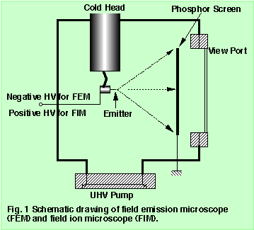
図1. FEMとFIMの模式図。
電界放射顕微鏡(FEM)は図1に示されるような装置で針状試料に負の高電圧を印加することにより試料表面の高電界から生ずる電界電子放射を蛍光板で観測する装置である。電界電子放射に必要な電界強度は109 V/mのオーダーであるので後述するFIM観察に必要な電界の10分の1程度の電界でFEM像を観察することが出来る。従って、試料先端の半径も数1000 nm程度で十分である。このような針状試料は金属ワイヤーを電解研磨することにより容易に作成することができる。FEM観察をおこなうためには試料先端が清浄表面でなければならないので、通常は試料を超高真空中で加熱して清浄表面を得た後に負の電界が試料に印加される。この場合、表面エネルギーの面指数依存性を反映したファセッテングが半球状の試料表面に生ずるので、これらのファセットした面の仕事関数と電界に依存する電流密度の差異から像コントラストが得られる(図2)。
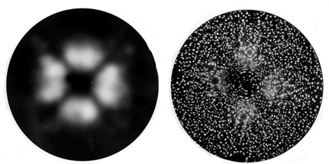
図2. Ni清浄表面から観察されたFEM像とFIM像。いずれの像も同一試料から得られている。

電界イオン顕微鏡(FIM)とは?
電界イオン顕微鏡(FIM)は1951年にペンシルバニア州立大学のErwin E. Mueller教授により発明された投影型の顕微鏡で、レンズを用いないので収差の影響を受けない。FIMにより人類は初めて原子を観察することに成功した。この顕微鏡は、電界放射顕微鏡(FEM)から発展した装置である。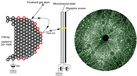
図3. 電界イオン顕微鏡(FIM)の原理を示した模式図。
図1で示したように装置の構成は非常に単純で、超高真空中に先端の直径が100 nm程度の先鋭な針を低温に保持し、その対面にマイクロチャネルプレートを装着している。試料表面は原子レベルでは図3に示されるように原子の配列による凸凹が生じており、これに高電圧を加えると原子が突き出た部分に高電界がかかる。そこにNeやHeなどの不活性ガスを導入すると、ガス原子は電界の高い部分でイオン化されてマイクロチャネルプレートに衝突し、その場所に輝点が生じる。つまりマイクロチャネルプレート上には針状試料表面の原子の凹凸を100万倍以上に拡大した像が得られる訳である。
FIMの装置自体はFEMと全く同じで、違いはFEMでは針に負の高電圧をかけるのに対して、FIMでは正の高電圧をかける。またFEMは超高真空中で像を観察するが、FIMは高電界下での結像ガスの電界イオン化現象を用いるので、 超高真空中にHe, Ne, H2などの結像ガスを10-3 Pa程度導入する必要がある。正の高電界がかかったときの金属表面のポテンシャルは図5(b)に示されるようになり、冷却により運動エネルギーを失った結像ガスが表面からxcの距離に達した時に、結像ガス原子は電子をトンネリングにより失いイオン化する。結像ガスの電界イオン化に必要な電界はHeで4.4 × 10¹⁰ V/m、Neで3.7 × 1010 V/m、H2で2.3 × 1010 V/m程度であるので、それを実現するための針 の曲率半径はFEMのそれよりも1桁低い50~100 nm程度のものが必要である。また結像ガスのイオン化による蛍光版の輝度はFEMに比べると著しく低いので、 FIMではマイクロチャネルプレート(MCP)という2次元のイメージ増倍管を用いて像を肉眼で観察できるようにしている。FIMが発明された当時は像は蛍光板で観察されていたので、像は完全な暗室内で全神経を集中させてみなければ観察できないほど暗かった。そのため、像撮影に長時間の露出が必要であり、蛍光効率の高いHeガスでの観察が可能なW, Mo, Pt, Rh, Ir, Reなどの高融点金属の観察しか行われなかった。
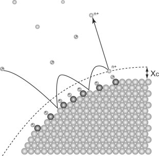
図4. 針状金属表面からの結像ガス原子の電界イオン化の模式図。
FIMの試料表面での電界イオン化の様子を図4に模式的に示す。試料は50 nm程度の曲率半径を持つ先鋭な針であり、その表面の原子レベルでの形態は図のようになる。 試料に高電界をかけると、分極した結像ガス原子が試料表面に引き寄せられて表面の電界の特に高い突出した原子に強く電界吸着していると考えられている。分極した原子が高い運動エネルギーで金属表面に引きつけられて衝突すると、試料が冷却されているのでガス原子は運動エネルギーを失いながら、跳ね返される。 跳ね返されたガス原子は再度表面に引き寄せられるというホッピングモーションを繰り返しながら徐々に熱エネルギーを失って、いずれガスが吸着している電界の高いところから図4で示されるxcの位置に来たときに、電子をトンネリングにより失って電界イオン化(Field Ionization)される。これらのイオンは試料表面と接地されたスクリーンの間の電界により加速されスクリーンに衝突し輝点が観察される。試料表面の電界分布は一様ではなく、図5中試料表面で黒く塗りつぶされたレッジやキンクの位置で原子が突出していて局所的に電界が高くなりガス原子の電界イオン化の確率が高くなる。毎秒103から104個の結像ガス原子がイオン化することによって、一つの輝点が形成されると考えられている。その結果これらの半球状の試料先端で突出した原子を蛍光板に投影した位置が明るく観察されることになる。
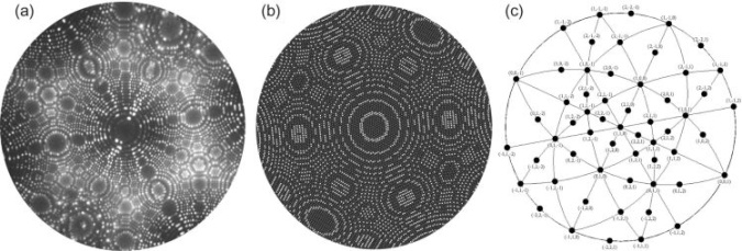
図5. (a) タングステンのFIM像と(b)(011)面を中心として半球状になった 表面原子の配位数の小さな原子を光らせた模型と(c) [011]晶帯軸のステレオ投影図。
像の倍率Mは試料とスクリーン間の距離をD、針の曲率半径をrとするとM = kD/rで与えられる。ここでkは投影中心の位置と増の広がりの補正項である。典型的なFIMの試料の曲率半径は50 nm程度であり、試料と蛍光板の距離は5 cmであるので像の倍率はおおよそ106倍程度になる。このようにFIMは投影型の顕微鏡であり、レンズにより像を拡大しないので、像は試料の振動やドリフトの影響を受けにくい。したがって装置の構成は非常に単純で、電子顕微鏡等で不可欠な除振機構が一切不要である。
FIMでは結像ガスの電界イオン化利用するので、FIM像を得るためにはイオン化電界以上の電界を試料表面に加えなければならない。ところが高電界では試料原子自体がイオン化される電界蒸発(Field Evaporation)とよばれる現象が生ずる。このため結像ガスのイオン化強度が試料の電界蒸発強度よりも低いことがFIM像を得るための条件となる。一般に高融点金属の電界蒸発強度は高い。低融点金属の場合、電界蒸発強度はHeガスのイオン化強度を下回るのでHeでの像観察ができない。そのような場合はイオン化強度の低い結像ガスを選ぶ。また電界蒸発は熱活性であるので、試料を極低温に冷却すれば、電界蒸発強度も上昇し、Heでの像観察も可能になる。
電界蒸発現象はFIMを可能とする重要な現象でもある。つまり、FIM用の針状試料は 従来金属線を電解研磨することにより得られるが、これらの表面は酸化被膜で覆われていた李、研磨ムラにより凹凸があったりする。しかし凸面では電界が高くなり、その部分で優先的な電界蒸発が進行するので、電界蒸発を行っていくと自己触媒的に原子的にスムーズな清浄表面ができる。またFIM像を観察しながら表面原子層を順次電界蒸発させることにより、試料表面から規則的に原子面を蒸発させて、試料の3次元的な観察が可能となる。後述のアトムプローブ分析法では高電圧パルスを同期させた電界蒸発を用いて原子のイオン化を行う。
図5に指数付けしたタングステンのHeによるFIM像と半球上の表面で突出した(配位数の少ない)原子を光らせたモデル、さらに[011]晶帯軸のステレオ投影図が示されている。 FIM像は半球状の表面原子を平面に投影したものであるので、 結晶面はほぼステレオ投影と同じ対象性と位置関係で現れてくる。 図5(b)に見られるような針状表面で突出している原子(配位数の少ない原子)を平板スクリーンに投影したのがFIM像であるので、低指数面のレッジの原子列はFIM像上では同心円状に見える。図5のタングステン像では低指数面では原子ステップを表す同心円状のパターンが観察されるだけであるが、高指数面においては個々の原子が分解されている。
FIM像解釈の基礎
FIM試料の先端は50 nm程度の曲率を持つ半球状の形になっている。前述のように試料形状は電界蒸発による自己制御によって決まる。結晶面の表面エネルギーに差があると、表面エネルギーの低い面の曲率半径は高い面にくらべて平坦になる傾向がある。また高温になればなるほど、このファセッテングが顕著になる。このように試料表面は理想的な半球状とならず曲率半径が結晶面によって若干異なってくる。したがって、像倍率も結晶面により異なる。このような試料表面の曲率半径は図6に示すように、おなじFIM像中の2つの指数面間の距離とその間の面の数から評価することができる。今、FIM像を観察して(011)極と(001)極の間に(011)面が何層あるかを数える。図6では(011)面が6原子層観察される。曲率半径と2つの面の間の角度には次のような関係が成り立つ。この関係から、例えば図6で試料をタングステンとすると、(011)極と(001)極の間で(011)面が6枚観察されるので、r = 6×0.224/(1-cos45°) = 4.5 nmということになる。
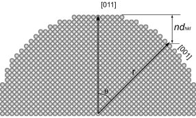
図6. FIM像からの試料半径の求め方。
様々な試料のFIM像の実例を示して、実際の金属材料がどのように観察されるかの理解の一助としたい。図7(a)は結晶粒界を含むタングステンのHeイオン像である。このように高融点金属では個々の原子を分解できるような高い質のFIM像が得られる。さらに結晶粒界を隔てて2つの結晶方位のFIM像が観察される。粒界部分は原子が完全に接触して見える部分と、暗く像が抜けている部分がみられる。後者はこの部分で試料表面に凹部があるためと考えられる。図7(b)は純アルミニウムのHeイオン像である。一般に低融点金属では面の表面エネルギーの差によって試料が大きくファセットするために、(001)面や(111)面での曲率半径が大きくなり、この部分での像が暗くなる。アルミニウム合金では(011)面の部分で試料が小さな曲率を持ち、像が最も明るく結像される。このような像のファセットはタングステンでも、試料観察温度を100 K程度に上げていくと観察される。図7(c)はGeを1at.%含むL12構造のNi3Al金属間化合物である。L12化合物の場合(011)面と(002)面はNiAl面とNi面の交互の積層になっているが、図7(c)にもみられるように、NiAl面はNi面に比べて暗く観察される。また電界蒸発強度の高いGe原子が(011)面のテラスに残って突き出しているためにこれらの原子4個が明るく観察されている。図7(d)時効処理したCr-20Fe合金で、Feのナノ析出物がCr母層中に析出している。FeはCrよりも蒸発電界が高いために、Fe析出物の部分が試料表面で突き出し、その結果、Fe析出物が母相に比べて明るく観察されている。析出物の蒸発電界が低い場合には全く逆のコントラストが現れる。図7(e)がその一例で、Al母相中に析出したAl3LiはLiの蒸発強度が低いために析出物のところで凹み、そのため析出物は母相に対して暗く観察される。図7(f)はSm(Co0.72Fe0.20Cu0.055Zr0.025)7.5焼結磁石のNeイオン像である。この試料にはSm2Co17母相と、相分解によって母相をセル状に囲むように形成されたSmCo5セル境界相、c軸に板状に析出するZ相の3相が存在している。明るく観察されているのが母相で、暗く観察されているのがセル境界相である。また試料の長手方向に垂直に析出している板状試料は、特に明るいコントラストをもったリングとして観察されている。このようなFIM像を得てから、原子をイオン化させてアトムプローブ分析を行うことにより、ここで観察されているようなナノ相の組成分析を行うことができる。
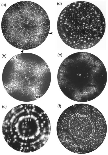
図7. 様々なFIM像。(a)タングステンの結晶粒界、(b)アルミニウムのHeイオン、(c)Geを含むNi3AlのNeイオン像、(d)Feの析出したCr-20at.%Fe合金のNe像、(e)Al3Liの析出したAl-6at.%Li合金、(f)Sm2Co17母相中に析出したSmCo5セル境界相とc軸に平行な板状Z相を含むSm(Co0.72Fe0.20Cu0.055Zr0.025)7.5焼結磁石のNeイオン像。
電界蒸発(Field Evaporation)とアトムプローブ
電界蒸発(Field Evaporation)は数V/nm程度の高い電界下で導電性物質の原子が表面からイオン化する現象である。数V/mという高い電界は先鋭な試料に高電圧を掛けてることによって実現可能な電界強度であり、実際には電界蒸発は電界イオン顕微鏡(FIM)や走査トンネル顕微鏡(STM)の探針でしか観察されない。図8の動画はタングステンのFIM像で、それに静的なFIM像が得られるよりも高い電圧を掛けたときに、FIM試料表面からタングステン原子が電界蒸発によってイオン化される様子を観察したものである。このような電界蒸発を高速の高電圧パルスを加えることによって起こさせ、電界蒸発したイオンが検出器に到達するまでの飛行時間を測定して質量分析を行うのがアトムプローブというわけである。
図8. タングステン表面からの電界蒸発を観察したFIM像(動画)。
アトムプローブ電界イオン顕微鏡
アトムプローブ電界イオン顕微鏡(APFIM)はFIMのスクリーンの中心にイオンが通り抜ける穴をあけて、このイオン飛行時間測定を行うことで、試料表面からイオン化される個々の原子を同定することによりサブナノメーター領域の濃度分析を行う装置である。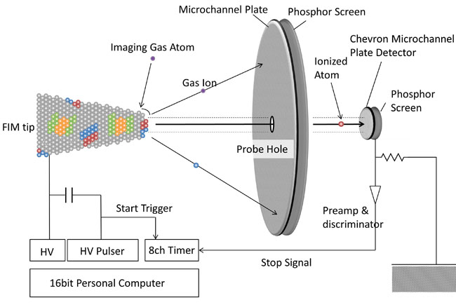
図9. アトムプローブ電界イオン顕微鏡(APFIM)の模式図。
FIM像で相のコントラストを観察し、分析したい領域をプローブホールで覆い、 FIM像観察に必要な電界よりもさらに高い電界を試料にかけると、試料表面の原子がイオン化される。このような原子の電界蒸発を高電圧パルスで行なえば、原子がイオン化される瞬間からこれが加速されて検出器に到達するまでの飛行時間を測定することができる。イオンのエネルギーは印加電圧から分かっているので飛行時間測定によりイオンの質量を決定することができる。原子は電界蒸発により試料表面から1原子層ずつイオン化されていくのでプローブホールで覆った領域の深さ方向の濃度プロファイルが測定できる。面内方向の分析の空間分解能はプローブホールの試料表面への投影径で決まり、これは試料半径と試料とスクリーンとの距離(FIM像の倍率)によって変化する。通常0.5 - 2 nm程度が実用的な面内方向の分解能である。一方で原子が1原子層ごとに蒸発するという性質を利用すれば深さ方向に1原子層(0.2 nm)の分解能を得ることができる。 さらにアトムプローブはイオンを飛行時間測定により同定するので、検出効率は原理的には質量(原子の種類)にかかわらず一定である。したがって水素、窒素、酸素、炭素、ボロンなどの実用材料で特に重要な軽元素の定量分析も可能なところに特長がある。
3次元アトムプローブ(3DAP)の原理
1988年にオックスフォード大学のA. Cerezoらにより開発された位置敏感型アトムプローブ(position sensitive atom probe; PoSAP)は、アトムプローブの検出器に位置敏感型検出器(position sensitive detector)を取り入れたもので、従来のアトムプローブで分析領域選択のために用いられていたプローブホールを用いずに、位置敏感型検出器に到達した原子の飛行時間と位置を同時に測定することのできる装置である。この装置を用いれば試料表面に存在する合金中の構成元素を原子レベルの空間分解能で2次元マップとして表示する事が出来るばかりでなく、電界蒸発現象を用いて試料表面を1原 子層ずつ蒸発させることにより、2次元マップを深さ方向に拡張していくことが可能となる。このデータをコンピュータで蓄積し再構成することにより、合金中の原子の分布を3次元的に再構成することができる。この手法は、従来のアトムプローブの分析領域がプローブホールのカバーする極めて微細な領域に限られるという欠点を克服しただけでなく、個々の原子の位置をサブナノメーターの分解能で決定することの出来るユニークな分析手法である。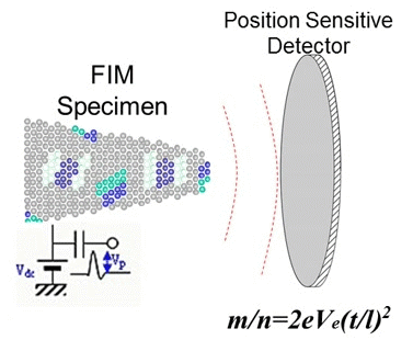
図10. 3次元アトムプローブの模式図(動画)。
位置敏感型アトムプローブでは、位置検出器の特性から同時に2個以上のイオンが検出器に到達した場合にはこれらのイオンの位置測定が不可能になるという欠点があるが、これを改善するためにフランスのルーアン大学のグループは位置検出器として100個の陽極を用いた多重検出システムを採用し、これを断層アトムプローブ(Tomographic Atom Probe; TAP)と名付けた。いずれにしてもイオンの飛行時間測定と位置検出を同時に行なうという点においてはPoSAPと原理的には同じであり、さらにこれらのデータを再構築することにより原子位置に関する3次元的な情報が得られるということで、これらのアトムプローブは総称して「3次元アトムプローブ(Three-Dimensional Atom Probe; 3DAP、またはAtom Probe Tomography; APT)」と呼ばれている。
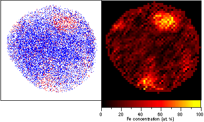
図11. 400 ℃で長時間熱処理されたCr-20Fe合金の3次元アトムプローブによる3次元元素マップと濃度マップ。
3次元アトムプローブにより得られた元素マッピングの例を図11に示している。分析領域はおおよそ20 x 20 nmであり、個々の点は原子が検出された位置を示している。青い点がCr原子、赤い点がFe原子に相当し、このデータからFe原子の集まった微細な析出物が分析領域内に存在していることが分かる。濃度マッピングは元素マッピングから各原子の個数を計算し、そこから0.4 x 0.4 nmをピクセルとして濃度の情報を示したものである。
このような2次元の元素マップを連続的に収集し、原子が収集される順序に比例するz座標を与えれば、図12のように、合金中の元素の3次元トモグラフィーを得ることができる。このように3次元アトムプローブを用いれば、これまでのどのような解析手法よりも高い分解能で原子の存在位置を決定することができるのである。
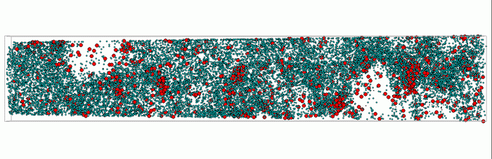
図12. Nd-Be-B-Cu合金から得られた3次元原子マップ(動画)。緑はNd原子、赤は銅原子を示す。
レーザーアトムプローブ
これまでの3次元アトムプローブ(3DAP)では静電界に数nsの電圧パルスを針状試料に加えて電界蒸発によって原子のイオン化を行うために、試料には導電性がなければならないという制約があった。このため、3DAPの応用は圧倒的に金属材料の解析に関するものである。10-2 Ohm·cm程度の高ドープSiや薄い酸化物層の電圧パルスによる解析例は報告されているものの、それ以上の抵抗率の試料の電圧パルスによる解析は不可能と考えられていた。さらに、現在一般的に使われている装置では、観察可能領域が縦横数10nm、深さ数100nm程度が限界であり、デバイス構造の解析にはより広領域の解析能が望まれている。また、実際の解析で最も問題となるのは、実は電界応力による試料の頻繁な破壊である。この事実はアトムプローブユーザー以外には一般に喧伝されていないが、多くの試料、特に転位などの欠陥を大量に含む金属系試料や多層膜などは、電圧パルスによる分析中に頻繁に破壊する。電界により針状試料先端にかかる応力は一般的な金属材料の降伏応力以上であり、このため電圧パルスによる分析ではデータ収集までに試料が頻繁に破壊され、試料によっては全く解析できないものもある。以上の3DAP法の制約はいずれも針状試料先端からので電界蒸発を利用してアトムプローブ法が可能となるという原理的な制約であるが、これらを克服できる可能性のある方法としてレーザー駆動による3DAP法(レーザーアトムプローブまたはレーザー補助3次元アトムプローブ)が注目されている(注:2000~2010年頃当時)。これまでの我々を含むいくつかのグループの実験により、パルスレーザーにより針状試料先端からの電界蒸発をアシストすると、
- イオン化の際にエネルギー欠損が無いため、エネルギー補償器無しの直線型アトムプローブであっても、質量分解能の向上が期待できる。
- その結果、飛行距離を短くできるので、検出器の開広角を従来の20倍以上に広角化できる。
- レーザーアシストの分だけ原子の蒸発電界強度を低く抑えられるので、試料破壊の頻度が著しく減少する。
- レーザー蒸発により、これまで不可能であった半導体の解析が可能になり、絶縁体解析の可能性もある。
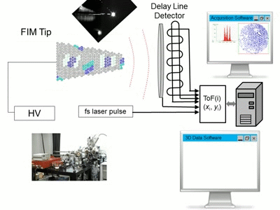
図13. レーザーアトムプローブの模式図(動画)。
図13にレーザーアトムプローブの原理の模式図を示す。従来装置で用いられていた高電圧パルスの代わりに、針状試料先端にフェムト秒レーザーパスルを照射することで電界蒸発のタイマーと同期させること以外は従来型の3次元アトムプローブ(電圧パルス型)と同じである。唯一の違いは、先に述べたように基本的にレーザーアシストによる 電界蒸発ではイオンのエネルギーが針状試料に加えられたDC電圧になるので、イオンにエネルギー欠損が生じない。 このために直線型であっても質量分解能が著しく改善されることから、試料・検出器間距離を短くすることができる。 結果として検出器の開口角を従来型のアトムプローブの20倍程度でできることが大きなメリットとなっている。
図14、図15は本センターで開発されたレーザーアトムプローブの模式図とその写真を示している。最近の研究(注:2000~2010年頃当時)により、質量分解能がレーザー照射条件によって大きく変わることが分かってきた。当初用いた波長1030 nmの赤外光レーザーでは試料によっては質量分解能が十分に得られない。これは長波長レーザーではフォノンを励起して試料温度が上昇し、その結果電界蒸発が起こるために、熱伝導の悪い試料で顕著に質量分解能が悪くなることが分かっている。そのため、図16に示す波長変換器を取り付け、現在の装置では2倍波の515 nmの可視光と3倍波の343 nmの紫外光レーザー、4倍波の257.5 nmを選択できるようにした。短波長レーザーでは電子励起によるイオン化が起こるためか、質量分解能が著しく改善されることが判明しており、この現象を用いて、我々は世界で初めてバルクのセラミクス材料のアトムプローブ解析に成功した。
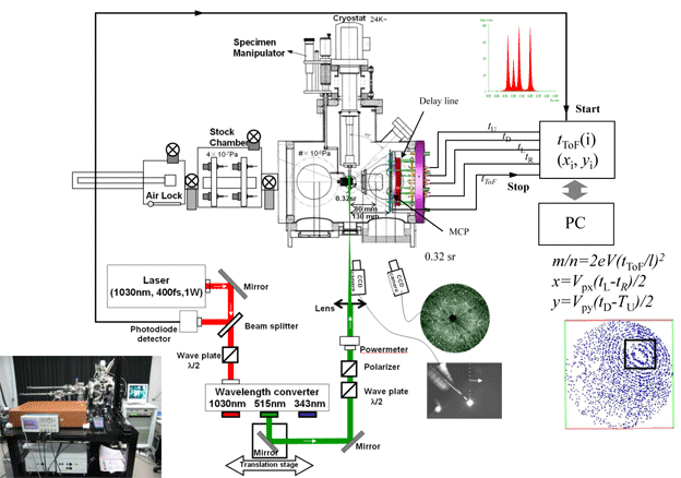
図14. NIMS設計のレーザーアトムプローブの模式図。
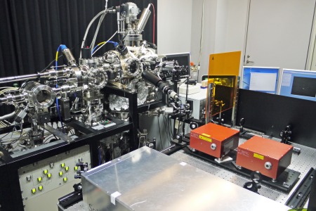
図15. NIMS独自開発レーザーアトムプローブ装置。
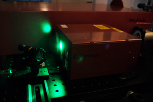
図16. NIMS独自開発レーザーアトムプローブ装置。
レーザー補助電界蒸発によりアトムプローブの応用範囲が爆発的に広がっており、同時にFIB-SEM複合装置を用いたマイクロサンプリング法により、任意領域からの分析も可能になっている。図17にはレーザーの短波長化により解析可能となった材料範囲をまとめている。
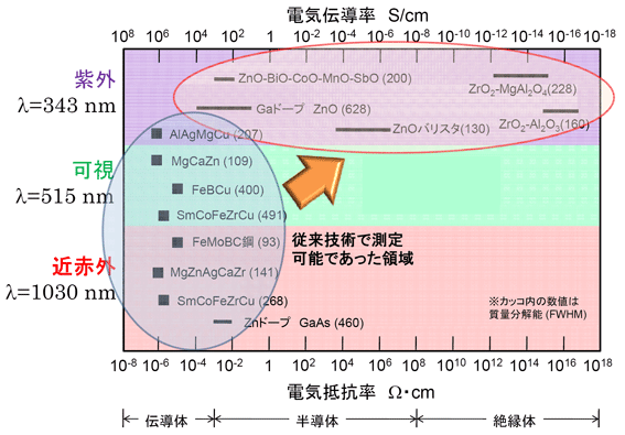
図17. レーザーの短波長化によりアトムプローブ解析可能となった材料範囲。
Principle of Field Ion Microscope (FIM)
Field ion microscope (FIM) was invented by Erwin E. Mueller in 1951 at the Pennsylvania State University. By FIM, man observed atoms for the first time. It was developed from its forerunner, the field emission microscope. The instrument features a specimen in the form of a sharp needle mounted on an electrically insulated stage that is cooled to cryogenic temperatures (20 to 100K) in an ultrahigh vacuum chamber (Fig. 1). The field ion image of the specimen is formed on a microchannel plate and phosphor screen assembly that is positioned approximately 50 mm in front of the specimen. To produce a field ion image, controlled amounts of image gas are admitted into the vacuum system. The type of image gas used depends on the material under investigation; common images gases are neon, helium, hydrogen and argon.Fig. 1. Principle of field ion microscope (FIM).
The field ion image is produced by the projection of image gas atoms that are ionized by the high positive voltage on the specimen onto the fluorescent screen. A schematic diagram of the multiple step imaging process is shown in Fig. 1. The image gas atoms in the vicinity of the specimen are polarized because of the high field and then attracted to the apex region of the specimen. After a series of collisions with the specimen during which the image gas atoms lose part of their kinetic energy, these image gas atoms become thermally accommodated to the cryogenic temperature of the specimen. If the field is sufficiently high, these image gas atoms are field ionized by a quantum-mechanical tunneling process. The ions produced are then radially repelled from the surface of the specimen towards the microchannel plate and screen assembly. A microchannel plate image intensifier positioned immediately in front of the phosphor screen produces between 103 and 104 electrons for each input ion. These electrons are accelerated towards the phosphor screen where they produce a visible image.
Field Evaporation & Atom Probe
Field Evaporation is the phenomena that atoms are ionized at the presence of extremely high electric field of the order of a few V/nm. Such high electric field can only be achieved by applying high voltage to a sharp needle like specimen. Thus, field evaporation can be observed only in Field Ion Microscopy (FIM) or scanning tunneling microscopy (STM). The movie of Fig. 2 shows field evaporating tungsten atoms from the tip apex surface of a tungsten specimen observed by FIM. The atoms start evaporation (ionization) when the electric field is much higher than the field to image FIM. Atom probe measures the time-of-flight of the ions field evaporated from the surface of FIM tip by controlled application of high frequency pulses.Fig. 2. FIM image (movie) observing field evaporation of tungsten atoms.
Atom Probe Field Ion Microscope (APFIM)
An atom probe field ion microscope (APFIM) is a combination of a field ion microscope (FIM) and a time-of-flight mass spectrometer of a single ion sensitivity. When high electric field is applied on a surface of a sharp needle tip, imaging gas atoms are ionized at the protruding sites on the surface. These ions hit the screen, forming brightly imaging spots. Hence, the FIM is a projection type microscope of an atomic resolution with an approximate magnification of a few million times. By applying higher electric filed, surface atoms of the specimen are also ionized. By this field evaporation process, one can sample atoms of the specimens from the surface. Measuring the time-of-flight of individual atoms which go through a small aperture in the center of the screen makes it possible to determine the mass to charge ratios of individual atoms. Atoms are collected only within the aperture. The effective size of the aperture is typically from 0.5 to 5 nm. Hence, atom probe has a spatial resolution of this dimension in the lateral direction. Atoms always evaporate from the surface, so the spatial resolution in the depth direction is a mono-atomic layer. A unique feature of the atom probe compared with the other analytical instruments is its extremely high spatial resolution and equal detection efficiency for light elements.Fig. 3. Principle of Atom Probe Field Ion Microscope (APFIM).
Principle of Three-Dimensional Atom Probe (3DAP)
In 1988, by applying for a position sensitive detector to a time-of-flight atom probe, Cerezo, Godfrey and Smith at the University of Oxford succeeded in determining both the mass to charge ratio (m/n) and the position of ions at the same time. They named this unique instrument a position sensitive atom probe (PoSAP), by which they showed it was possible to draw two-dimensional element mapping with a sub nanometer spatial resolution. Reconstruction of a series of two-dimensional element mappings with a graphics workstation made it possible to draw a three-dimensional element mapping in a 3D volume of a few nanometers' region. Later, a group of University of Rouen developed a similar atom probe using a multiple-anode detector, which can detect multi-event of iron arrival at the detector. This atom probe was named as a tomographic atom probe (TAP), because it can reveal the tomographic image of atoms in metallic materials. In essence, both atom probes use a position sensitive detector and can determine the mass to charge ratios and the positions of atoms in conductive materials, which enabled us to observe atom distributions in metallic materials in a3D space of a few tens' nanometer dimensions. Hence, these are generally called a three-dimensional atom probe (3DAP). Recently, the atom probe community used a term, three-dimensional tomography, more preferably.Fig. 4. Principle of 3DAP.
Examples of element and concentration mapping obtained by a PoSAP are shown in Fig. 5. In the element mapping, individual Fe atoms are shown by red dots, and individual Cr atoms are shown by blue dots. By counting the number of atoms in each pixel, the element map can be converted to a concentration map, where the concentration in each pixel approximately 0.4 x 0.4 nm is shown by a color scale. The observed area corresponds to approximately 20 x 20 nm.
Fig. 5. Element and concentration map of an aged Cr-Fe alloy. Red dots correspond to Fe atoms, and blue dots correspond to Cr atoms.
By sequentially collecting the two-dimensional elemental map as shown in Fig. 5, 3D atom tomography can be constructed as shown in Fig. 6. This technique has atomic resolution in sensitivity as a tomography method, and the spatial resolution is usually better than 0.2 nm though this value varies depending on specimen morphology and difference in evaporation field.
Fig. 6. Atom probe tomography of Nd and Cu atoms in a nanocrystalline Nd-Be-B-Cu alloy. The green and red spheres correspond to Nd and Cu atoms, respectively.
Laser-assisted 3D Atom Probe (3DAP)
In the conventional atom probe, atoms on tip apex were field evaporated by the application of ns high voltage pulsed on DC standing voltage. This requires specimens to be electrically conductive. Because of this principal limitation, the major application areas for the atom probe technique were metals. Some investigations reported the analysis of high doped Si of 10-2 Ohm・cm or thin oxide film layers. However, it was thought that the analysis of the materials with the higher electrical resistivity was impossible. Moreover, the most difficulty of the atom probe analysis comes from the frequent specimen rupture which is caused by the repetitive filed stress on the tip apex. Even metals, some materials like martensitic steels were extremely difficult to analyze due to frequent specimen rupture. In general, the field stress applied to tip apex is higher than yield stress of standard materials. This causes frequent specimen rupture using voltage pulses.In order to overcome such principal limitations of the atom probe technique, laser assisted field evaporation has been proposed. Attempts of laser assisted field evaporation were made in 1970's by various groups, but due to the limited performance of the laser systems in those days, laser assisted atom probes have been obsolete till recently. The Rouen group has revived the laser assisted atom probe in 2004 by employing femto second pulsed laser to their tomographic atom probe. Thereafter, several groups implemented either pico or femto second lasers to 3D atom probe, and it is now established that laser assisted field evaporation widens the application areas of atom probe tomography in various types of materials including metals, semiconductors and their devices. Several attempts have been made to analyze insulator materials like MgO in tunneling junctions of some other metallic oxides, but all of the successful reports of insulator analysis were on thin films.
Fig. 7. Schematic illustration of laser assisted 3D atom probe (3DAP).
As shown in Fig. 7, the laser assisted 3D atom probe is the same as the standard 3D atom probe except that atoms are field evaporated by the irradiation of laser pulses. Since voltage pulses are not applied to the tip apex, the field stress is substantially alleviated, so the chance of tip rupture can be substantially decreased. Since energy deficit is not expected by the laser triggered field evaporation, the mass resolution of the time-of-flight mass spectroscopy is expected to be substantially improved. However, currently available experimental results suggest that time delay occurs by the laser triggered field evaporation due to the time lag of the thermal conductance in poor conductive materials. However, our recent studies have shown that the mass resolution can be substantially improved by employing short wavelength (UV: 355 nm) femto second (400 fs) laser pulses. This indicates that the field evaporation mechanism is not a simple thermal mechanism when short wavelength laser is employed. Since the mass resolution can be improved substantially, it is possible to keep the flight distance short (~15 cm) so that a large acceptance angle (~0.3 sr) can be kept. Accordingly, a large angle of view can be achieved in laser assisted 3DAP compared to the conventional 3D atom probe (both straight and energy compensated atom probe). We have also found that the employment of short wave length laser (355 nm) makes the field evaporation of insulator ceramics possible, thereby even bulk insulator ceramics can be analyzed with the laser assisted 3D atom probe.
Fig. 8. Schematic illustration of the laser assisted wide angle 3D atom probe at NIMS.
Fig. 9. fs-laser-assisted 3DAP developed by NIMS.
Since the laser assisted 3D atom probe has been proven to be superior to the conventional voltage mode 3DAP, this will become standard soon (* Note in Dec. 2025: The most of recent reported 3DAP studies were used by laser assisted type.). It can analyze wide variety of materials including metals, semiconductors, and ceramics with less chance of specimen rupture. Although metallic materials have been analyzed with the voltage mode, our study indicated that there is no demerit of employing laser compared to voltage pulses even for metallic materials. Therefore, the laser assisted 3D atom probe will become the standard instrument for nano analysis and atomic tomography of all types of inorganic materials.