- Home
- > Research
- > Research Highlights
- > Vol. 65 New Laser-Assisted Non-Volatil・・・
 Research Highlights
[Vol. 65]
New Laser-Assisted Non-Volatile Memory Based on 2D van-der-Waals Heterostructures
- Previous
- Index
- Next
17 Mar, 2021
A research team at MANA has demonstrated a laser-assisted non-volatile memory device based on two-dimensional van-der-Waals heterostructures.
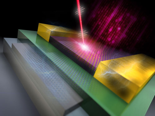
The researchers designed and investigated a few-layer rhenium disulfide (ReS2) field-effect transistor with a local floating gate (FG) of monolayer graphene separated by a thin hexagonal boron nitride (h-BN) tunnel layer and applied it to non-volatile memory (NVM) devices.
FG-NVM devices based on 2D van-der-Waals heterostructures (atomically thin layers that are attached to each other via very weak van-der-Waals interactions) have been the focus of considerable attention recently, as their tuneable and multibit operation under laser light could make them important components in future digital electronics and multifunctional memory applications.
The team demonstrated multi-level memory operation via 532nm laser pulse and electrostatic gate pulse coupling. The robustness and stability of the laser-assisted tuneable ReS2/h-BN/FG-graphene device show the potential for multibit information storage.
Laser-assisted memory operation provides a new degree of freedom for multifunctional optoelectronic devices with the extra functionality of optically communicated multilevel access. Since laser light can travel through free space without losing power, it allows operation of optoelectronic devices from a distance at low power and with little need for maintenance.
The MANA researchers used direct bandgap multilayer ReS2 because the material satisfies various requirements as a channel material for electronic devices, as well as being a strong light-absorbing layer, which makes it useful in light-assisted optoelectronic applications.
The device exhibits the functionality of a conventional electronic memory and can store laser-pulse excited signal information for future all-optical logic and quantum information processing.
It also addresses a need for a low power and optical control of multi-level operation of NVM devices, as well as for an NVM optoelectronic device that can distinguish light wavelengths for color sensing in digital imaging.
This research was carried out by Yutaka Wakayama (Group Leader, Quantum Device Engineering Group) and his collaborators.
Reference
“Laser-Assisted Multilevel Non-Volatile Memory Device Based on 2D van-der-Waals Few-Layer-ReS2/h-BN/Graphene Heterostructures”
Author: Bablu Mukherjee, Amir Zulkefli, Kenji Watanabe, Takashi Taniguchi, Yutaka Wakayama and Shu Nakaharai
Journal: Advanced Functional Material 30 [42] 2001688 [25 August 2020]
DOI: 10.1002/adfm.202001688
(Press release on this research)
"Development of a Multivalued Optical Memory Composed of Two-Dimensional Materials” (25 August 2020)
https://www.nims.go.jp/eng/news/press/2020/08/202008250.html
(MANA E-BULLETIN)
https://www.nims.go.jp/mana/ebulletin/
Affiliations
International Center for Materials Nanoarchitectonics (WPI-MANA), National Institute for Materials Science (NIMS), Namiki 1-1, Tsukuba, Ibaraki 305-0044, Japan
Contact information
Research Center for Materials Nanoarchitectonics (MANA)
National Institute for Materials Science
1-1 Namiki, Tsukuba, Ibaraki 305-0044 Japan
Phone: +81-29-860-4710
E-mail: mana-pr[AT]nims.go.jp
1-1 Namiki, Tsukuba, Ibaraki 305-0044 Japan
Phone: +81-29-860-4710
E-mail: mana-pr[AT]nims.go.jp