Major Equipments
★当センターの研究活動で使用されている主要装置です。超高真空クラスタースパッタ成膜装置 - Ultra High Vauum Cluster-type Sputtering Deposition System -
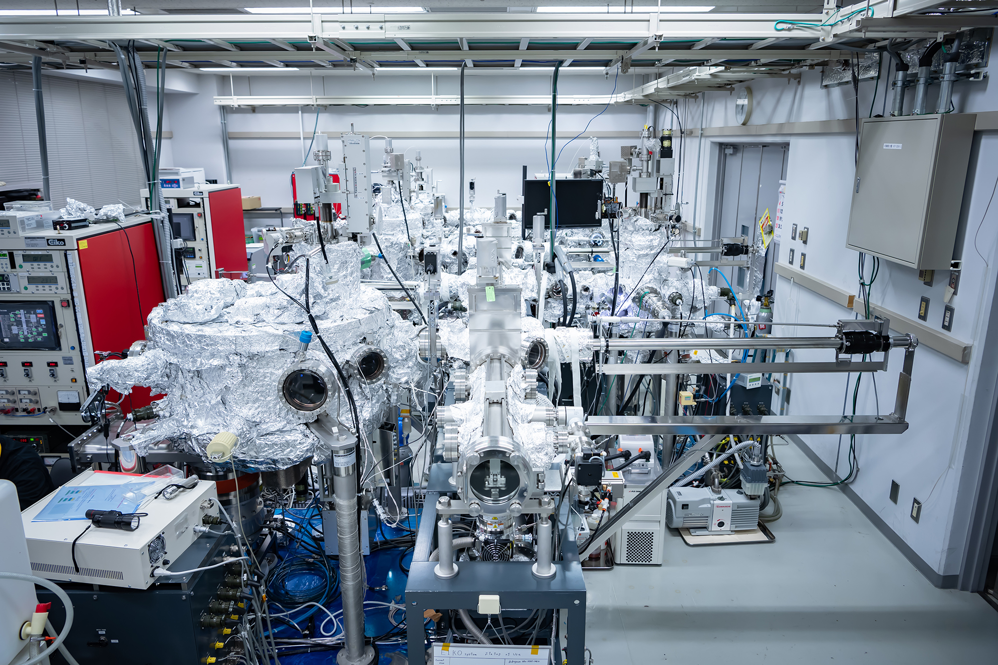
トランスファーチャンバで結合された複数の超高真空スパッタ成膜チャンバーを有する成膜装置。大気暴露をすることなく最大で18元ソースを利用した成膜が可能です。本装置によって作製した高品位な巨大磁気抵抗素子において世界最高レベルの磁気抵抗特性を実現しています。
UHV sputtering deposition system which has two sputtering chambers connected by the transfer chamber. Maximum 18 source can be deposited without air exposure in this system. High quality giant magnetoresistive device made by this system successfully realized the highest record of magnetoresistive property in the world.
UHV sputtering deposition system which has two sputtering chambers connected by the transfer chamber. Maximum 18 source can be deposited without air exposure in this system. High quality giant magnetoresistive device made by this system successfully realized the highest record of magnetoresistive property in the world.
時間分解磁気光学カー効果測定装置 - Time resolved magneto-optical Kerr effect (TRMOKE) -
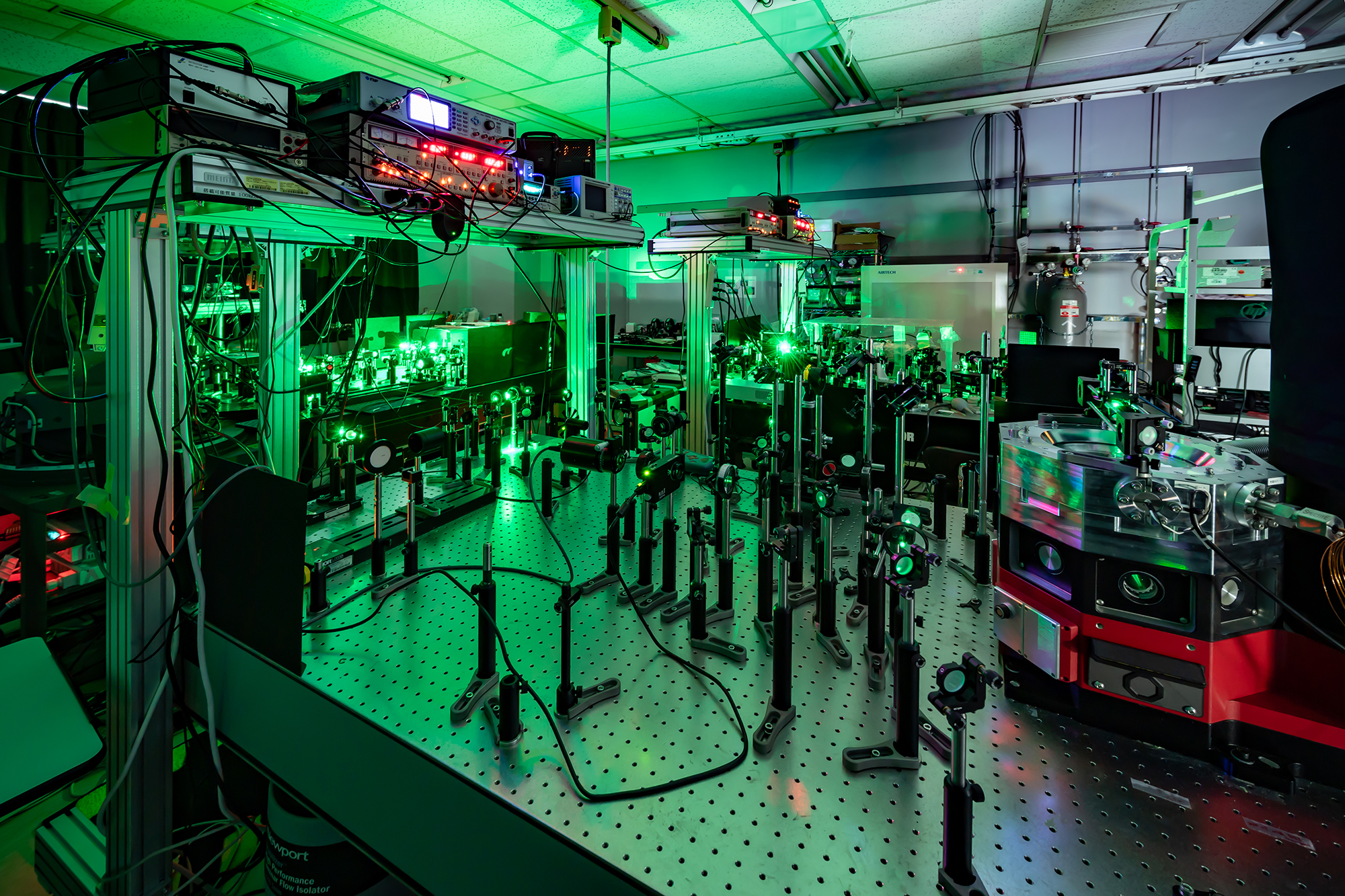
磁気光学カー効果は、光が磁性材料の表面で反射する際、磁性材料の磁化状態に応じて偏光状態が変わる現象です。これを応用することで、磁化状態の変化を観察することができます。特に、ポンプ光によって励起された磁性材料の磁化ダイナミクスをプローブ光の磁気光学カー効果を介して測定する方法を時間分解磁気光学カー効果(TRMOKE)と呼びます。電気的計測装置だけを用いた一般的な測定手法では観測できない超高速な磁化ダイナミクスを計測・解析できます。
The magneto-optical Kerr effect is a phenomenon in which the polarization changes when light reflects on the surface of a magnetic material, depending on the magnetization state. By applying this, it is possible to observe the magnetization dynamics. In particular, time resolved magneto-optical Kerr effect (TRMOKE) is a measurement technique of the magnetization dynamics, excited by pump laser pulse, through the polarization change of the probe laser pulse. This allows us the observation of ultra-fast magnetization dynamics that cannot be observed with conventional measurement methods using only electrical devices.
The magneto-optical Kerr effect is a phenomenon in which the polarization changes when light reflects on the surface of a magnetic material, depending on the magnetization state. By applying this, it is possible to observe the magnetization dynamics. In particular, time resolved magneto-optical Kerr effect (TRMOKE) is a measurement technique of the magnetization dynamics, excited by pump laser pulse, through the polarization change of the probe laser pulse. This allows us the observation of ultra-fast magnetization dynamics that cannot be observed with conventional measurement methods using only electrical devices.
球面収差補正走査型透過電子顕微鏡 - Cs-corrected Scanning Transmission Electron Microscope (S/TEM) -
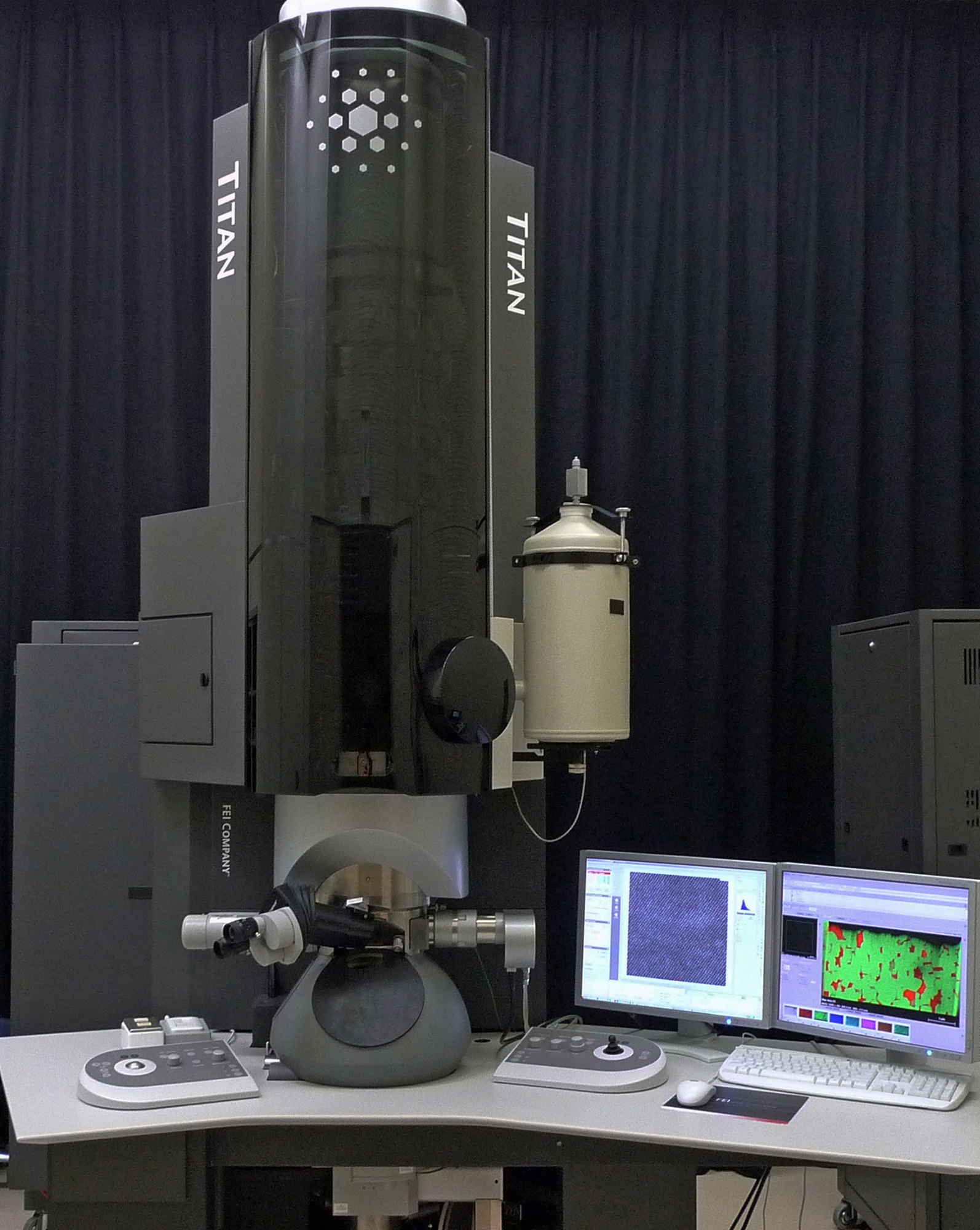
球面収差補正(Cs-corrected)により電子線を非常に小さく収束させ、原子間距離を下回る0.08 nmの空間分解能を有しています。単原子レベルでの構造観察や、EDS(Energy Dispersive x-ray Spectroscopy)、EELS(Electron Energy-Loss Spectroscopy)等元素分析が可能な高分解能走査型透過電子顕微鏡(S/TEM)です。
Titan G2 80-200 S/TEM (FEI) can be operated at 80-200 kV. Cs correction make electron probe much smaller, and it enables the microscope to get a higher-resolution (below 0.08nm). The microscope also support chemical analysis such as EELS (Electron Energy-Loss Spectroscopy), EDS (Energy Dispersive x-ray Spectroscopy) with atomic resolution.
Titan G2 80-200 S/TEM (FEI) can be operated at 80-200 kV. Cs correction make electron probe much smaller, and it enables the microscope to get a higher-resolution (below 0.08nm). The microscope also support chemical analysis such as EELS (Electron Energy-Loss Spectroscopy), EDS (Energy Dispersive x-ray Spectroscopy) with atomic resolution.
局所電極型レーザーアトムプローブ - Local Electrode Atom Probe "LEAP5000XS" -
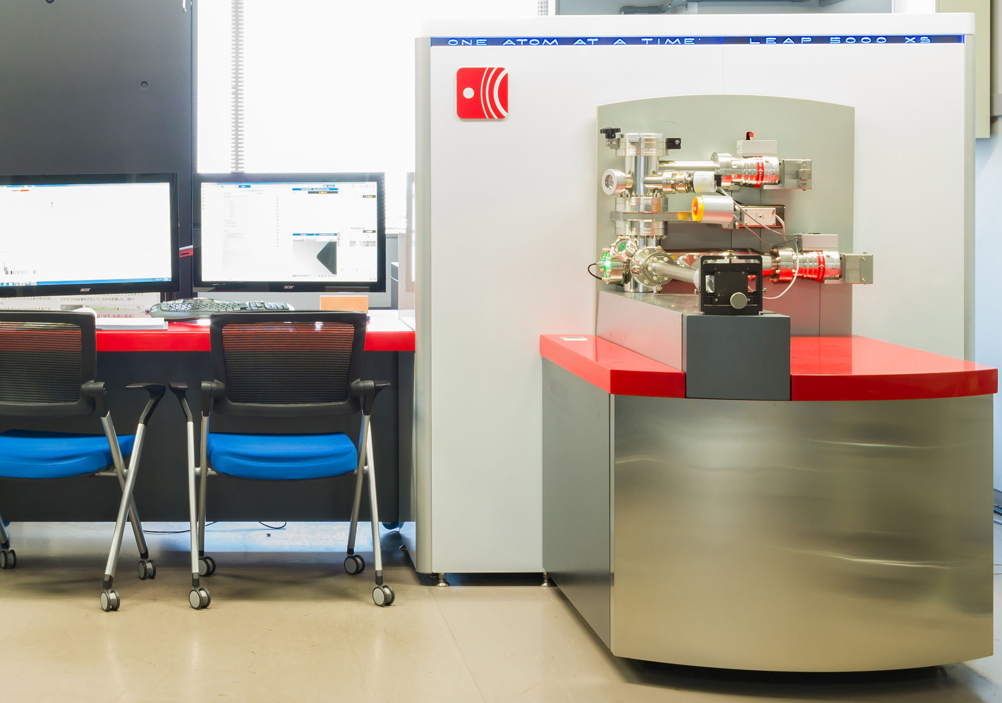
3次元アトムプローブは、電子顕微鏡では分析のできない軽元素を含む全ての元素について個々の原子の同定と位置決定ができるユニークな分析装置で、さまざまな材料やデバイス中の元素分布の3次元解析に威力を発揮します。3次元アトムプローブ法は、針状試料の先端からレーザーでイオン化される原子の質量と位置を同時計測することにより、100万倍以上の倍率で原子分布を3次元マップとして可視化できる唯一の手法です。LEAP5000XSは、紫外レーザパルスモード搭載型ストレートパスです。
The 3D atom probe method is the only method to visualize the distribution of atoms as 3D map at a magnification ratio of over 1 million by simultaneously measuring the mass and position of atoms ionized with lasers from the tip of a needle-shaped sample. For example, this method can precisely analyze the distribution of elements within a nanoscale device or the uneven distribution of nanoscale elements within a material. The "LEAP5000XS" is straight flight path with 355 nm UV laser pulsing atom probe system. Transferring 3DAP samples between FIB-SEM and 3DAP machine kept at low temperature and without air exposure is possible by using VCTM (Vacuum and Cryo Transfer Module).
The 3D atom probe method is the only method to visualize the distribution of atoms as 3D map at a magnification ratio of over 1 million by simultaneously measuring the mass and position of atoms ionized with lasers from the tip of a needle-shaped sample. For example, this method can precisely analyze the distribution of elements within a nanoscale device or the uneven distribution of nanoscale elements within a material. The "LEAP5000XS" is straight flight path with 355 nm UV laser pulsing atom probe system. Transferring 3DAP samples between FIB-SEM and 3DAP machine kept at low temperature and without air exposure is possible by using VCTM (Vacuum and Cryo Transfer Module).
FIB-SEM複合装置 - FIB-SEM Dual Beam "Helios5UX"/"CrossBeam550L"/""HeliosG4UX"/"CrossBeam1540EsB" -
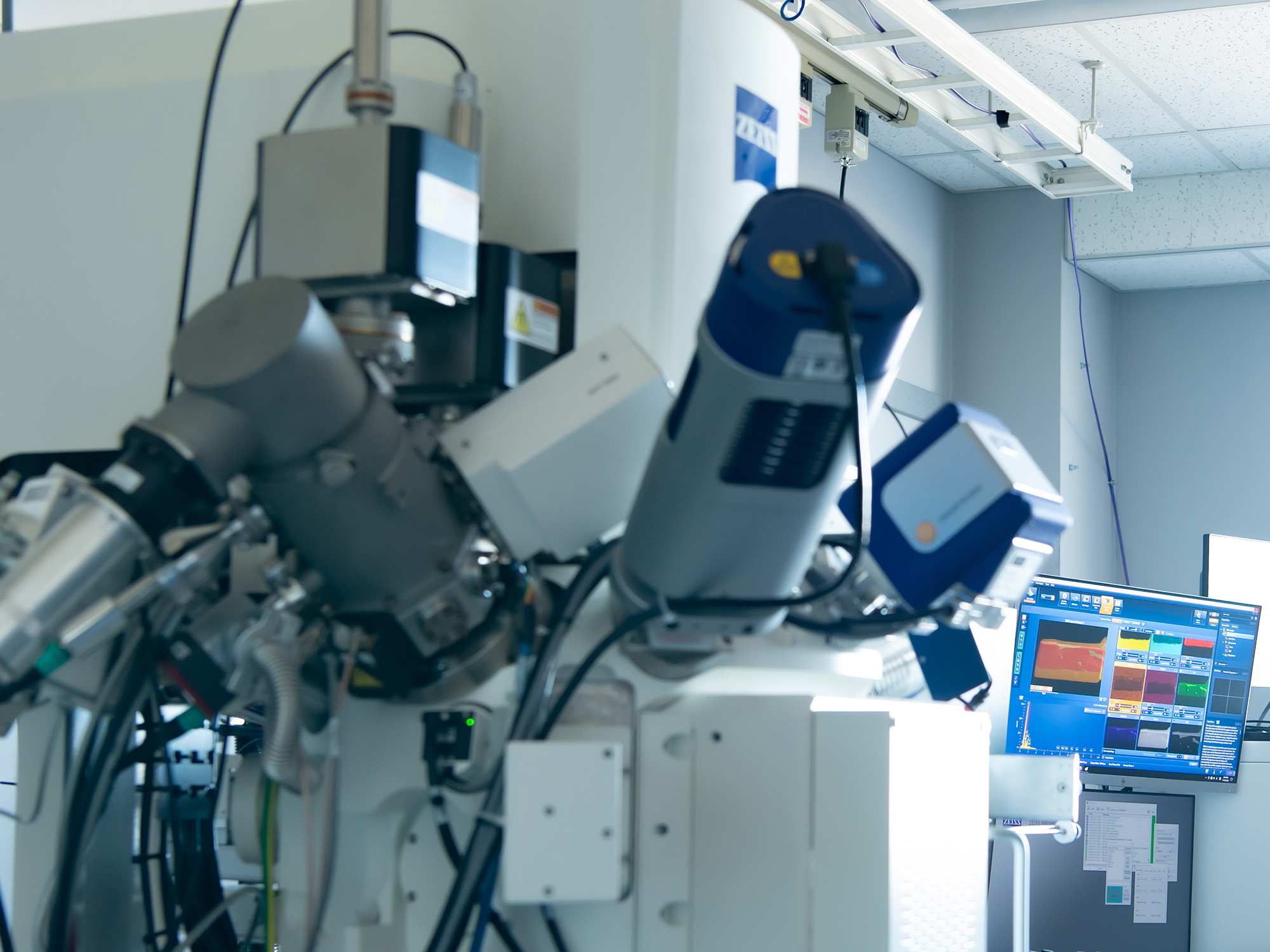
微細加工(FIB; Focused Ion Beam)と観察(SEM; Scanning Electron Microscope)の複合装置で、SEM観察、EDS元素分析、EBSD方位解析、SEMトモグラフィーに加えて、マイクロマニピュレーターを用いたマイクロサンプリング法により、試料の任意領域からTEM/3DAP試料を作製することができます。結晶粒界、複相組織の異相界面、多層膜の界面、デバイスの任意領域のナノ組織解析を可能にします。
The system combines microfabrication (FIB; Focused Ion Beam) and observation (SEM; Scanning Electron Microscope) capabilities. In addition to SEM observation, EDS elemental analysis, EBSD crystal orientation analysis, and SEM tomography, it enables the preparation of TEM/3DAP specimens from ROIs of the samples using lift-out method with a micromanipulator. The samples fabrication technique enables nano-structural TEM/3DAP analysis of grain boundaries, phase interfaces in multi-phase structures, interfaces in multilayer films, and ROIs within devices.
The system combines microfabrication (FIB; Focused Ion Beam) and observation (SEM; Scanning Electron Microscope) capabilities. In addition to SEM observation, EDS elemental analysis, EBSD crystal orientation analysis, and SEM tomography, it enables the preparation of TEM/3DAP specimens from ROIs of the samples using lift-out method with a micromanipulator. The samples fabrication technique enables nano-structural TEM/3DAP analysis of grain boundaries, phase interfaces in multi-phase structures, interfaces in multilayer films, and ROIs within devices.