Nanostructure Image Gallery
3D elemental map of Bulk Insulator Ceramics
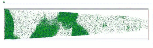
Contrary to the popular belief that bulk insulators cannot be analyzed by the atom probe technique, we have demonstrated that atom probe analysis of bulk insulating ceramics is possible by using ultraviolet femtosecond pulse laser. For the demonstration, spark plasma sintered yttria-stabilized ZrO2-MgAl2O4 nanocomposite material was used. Needle like specimens for field ion microscopy and atom probe analysis were prepared from the bulk sample using the focused ion beam technique. Three dimensional elemental distributions from both the zirconia and spinel have clearly demonstrated that the laser assisted field evaporation yield quantitative atom probe tomography. Atom probe tomography of Al (green) and Mg (blue) atoms with a volume of ~65×65×270 nm3. The grain boundary segregation of Al and Mg can be clearly seen on the right-hand side. © Y.M. Chen, T. Ohkubo, M. Kodzuka, K. Morita and K. Hono, 2009
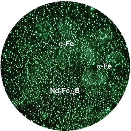
3D elemental map of Nd-enriched grain boundary in a Dy-diffused Nd-Fe-B sintered magnet
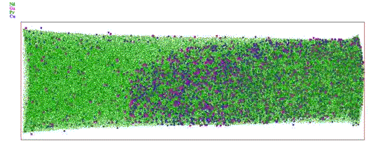
The above 3DAP elemental map shows the distributions of Nd (green), Ga (purple), and Cu (blue) atoms. A grain boundary can be clearly visible from the difference in the orientation of the lattice planes. The grain boundary is enriched with Nd, Ga and Cu. Both Cu and Ga are segregated at the interfaces between the Nd-rich grain boundary phase and the Nd2Fe14B grains. © H. Sepheri-Amin, T. Ohkubo and K. Hono, 2010
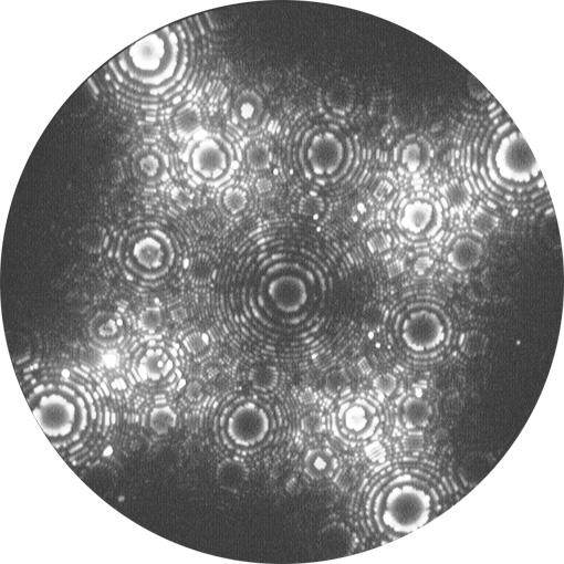
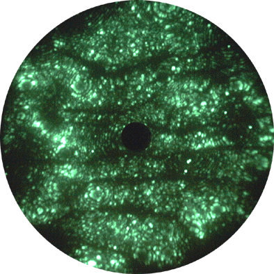
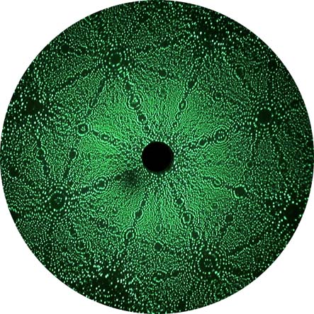
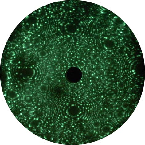
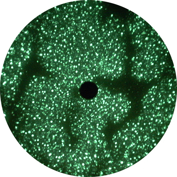
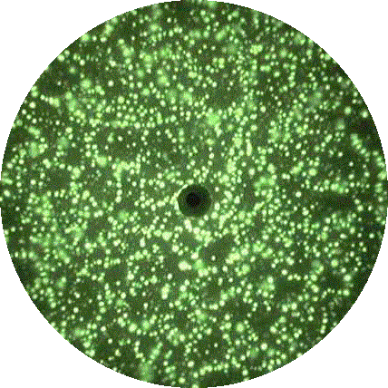
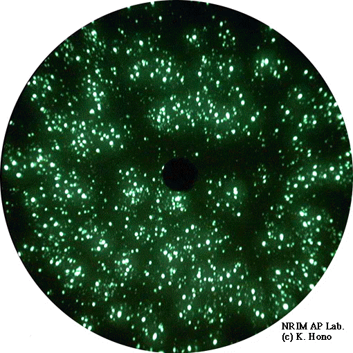
Images of FIM (Field Ion Microscope)
| Pure Al | Heavily drawn pearlitic steel wire | Low temperature Ne image of Ni3Al | Ferrite in Fe-0.11C-0.42Mn-0.31Si-0.5Mo (wt.%) Low Carbon Steel |
 © K. Hono, 1999 |
 © H.G. Read and K. Hono |
 © K. Hono |
 © W.T. Reynolds and K. Hono |
| Since the evaporation field of aluminum is around 30 V/nm, observation of FIM image of aluminum used to be thought difficult. However, by cooling specimens below 30K, clear FIM images of aluminum can be obtained as demonstrated here. The image was observed using He as an imaging gas at 28 K at a tip voltage of 5 kV. | Ne field ion image of Fe-Mn-Si-C pearlitic steel wire with a deformation strain of 4.22. Specimen courtsy of Dr. Tarui, Nippon Steel. | Ne field ion image of Ni75Al24Fe1 specimen observed at 20 K. | Ne field ion image of the ferrite phase in Fe-0.11C-0.42Mn-0.31Si-0.5Mo (wt.%) low carbon steel. |
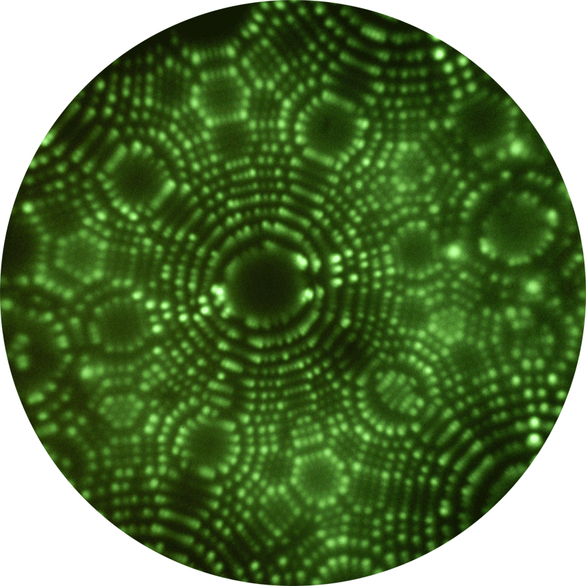
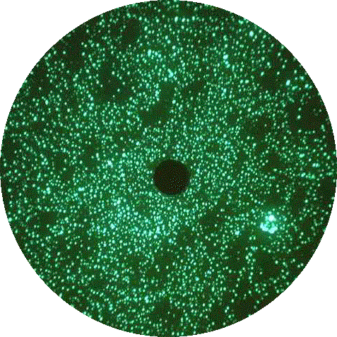
| Fe-4.5Nd-18.5B-3Co-1Ga melt-spun alloy crystallized at 700 C for 10 min. | FINEMET | Fe/Nd2Fe14B nanocomposite | Standard FIM image of W (tungsten) |
 © D.H. Ping and K. Hono |
 © K. Hono |
 © Y.Q. Wu and K. Hono |
 © K. Hono |
| Ne field ion image of Fe-18.5B-4.5Nd-3Co-1Ga melt-spun alloy annealed at 700 C for 10 min. Darkly imaging region is Nd12Fe82B6 hard magnetic phase and the brightly imaging region is the Fe3B phase. | Ne field ion image of Fe-13.5B-9B-3Nb-1Cu melt-spun alloy annealed at 500 C for 60 min (FINEMET). Darkly imaging region is the bcc-FeSi nanocrystalline particles and the brightly imaging region is the residual amorphous matrix phase. FINEMET is a pioneering material as nanocrystalline soft magnetic materials. | Ne field ion image of Fe/Nd2Fe14B nanocomposite hard magnetic material. | Standard FIM image of tungsten (W). |
| Rapidly solidified Al-V-Fe | GP zone in Al-4Ag alloy | Al-1.7Mg-1.1Cu alloy aged at 150 C for 5 min. | Rapidly solidified Al-4Ni-8Sm alloy annealed at 225 C for 1 h. |
 © K. Hono |
 © M. Murayama and K. Hono |
 © L. Reich and K. Hono |
 © T. Gloriant, D.H. Ping and K. Hono, 1998 |
| Ne field ion image of an rapidly solidified Al-4V-2Fe alloy. The darkly imaging region is a crystallized Al, and the brightly imaging region is V and Fe enriched amorphous phase. Note that the fcc phase is interconnected. With curtsy of Prof. A. Inoue, IMR, Tohoku University for specimen provision. | FIM image of Al-4Ag alloy aged at 150 C for 15 hours observed at 30 K using an imaging gas of He and Ne mixture. The brightly imaging regions are Ag-enriched GP zones. | He field ion image of Al-1.7Mg-1.1Cu alloy aged at 150 C for 5 min. | FIM image of an rapidly solidified Al-4Ni-8Sm alloy annealed at 225 C for 60 min. The image was obtained using a mixture of Ne and He as an imaging gas. The darkly imaging region is fcc Al, and the surrounding brightly imaging region is Ni and Sm enriched amorphous matrix. As the matrix is amorphous, no regular arrangement of bright sponts can be seen. The intensely bright region is a particle of some intermetallic compound. |
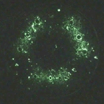
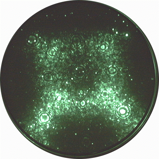
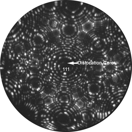
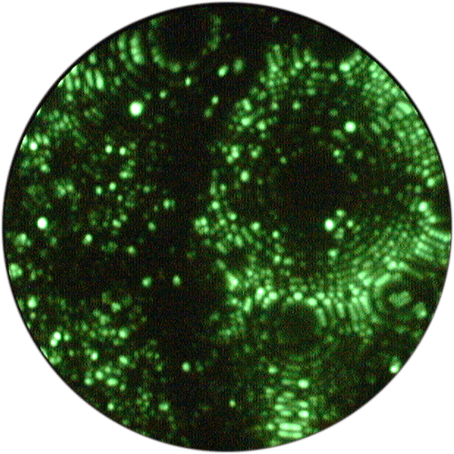
| Dislocation in an IF steel | Grain boundary in an IF steel | Inconel X-750 | Sm(Co,Fe,Cu,Zr) magnet |
 © K. Hono |
 © K. Hono |
 © T. Honma and K. Hono, 2001 |
 © X. Xiong and K. Hono |
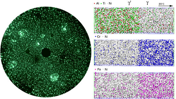
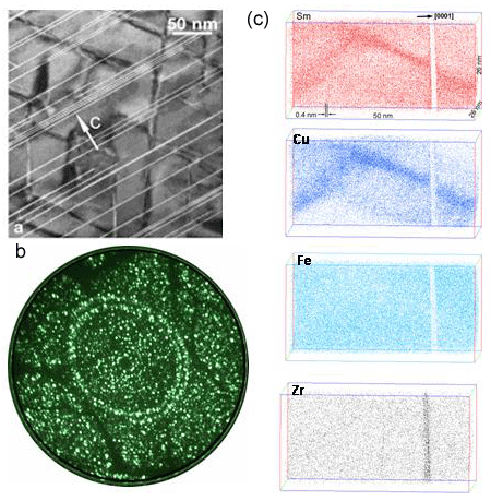
| Ne field ion image of an interstitial free steel containing a dislocation. Specimen courtesy: Kawasaki Steel. | Ne field ion image of a grain boundary in an interstitial free (IF) steel. | Ne field ion image of Inconel X-750 superalloy (Ni-16.1Cr-6.5Fe-2.9Ti-1.5Al (at.%)) and 3DAP elemental maps of Al, Ti, Cr, Fe and Ni atoms. Brightly imaging particles in the FIM image are gamma' particles. The 3DAP data show atom distributions at gamma'/gamma interface. In the gamma' phase, atomic layer can be resolved corresponding to the periodical atomic stacking on the (002) planes. Ti and Al rich planes and Ni planes alternately appear in the [001] direction. | Sm(Co0.72Fe0.20Cu0.055Zr0.025)7.5焼結磁石のTEM像、FIM像、3DAPによる元素マップ。TEM像にみられるようにこの磁石合金にはセル相、セル境界相、板状析出物の3相が混在している。FIM像の中心に同心円状にみえる面はSm2Co17相であり、それを円環状に囲んでいる明るい相はc面に板状に析出したZ相。暗く見える境界相はセル境界相のSmCo5。3次元アトムプローブによる元素分布でもこれらの相が明瞭に識別できる。 |