1. Home
  2. > Research
  3. > 2D Quantum Materials Group

Research2D Quantum Materials Group

Nanoscience and nanotechnology of low-dimensional materials

Electrons and phonons confined in low-dimensional nanostructures respond differently to external stimuli, leading to phenomena that are distinctly different from those in bulk materials. Low-dimensional nanostructures, therefore, provide a fascinating platform for exploring novel phenomena. In order to explore the possibilities of low-dimensional nanostructures, our research activities have focused on

1. Fabrication of low-dimensional nanostructures using advanced thin film growth techniques
2. Structural analysis and local electronic structure characterization using microscopy techniques
3. Exploration of novel phenomena through optical/electronic property measurements

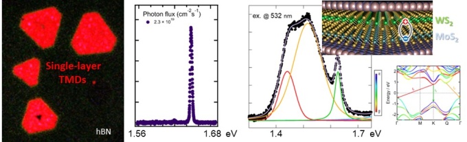
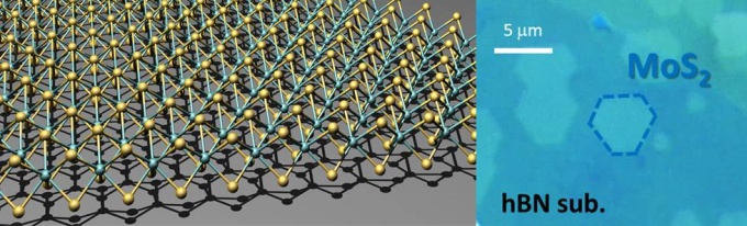
We work on various one- or two-dimensional nanomaterials, including carbon nanotubes, graphene, transition metal dichalcogenides and their heterostructures. The growth of high-quality samples, the fabrication of nanodevices, and the optical/electronic characterization are the core of our research. Our goal is to open up the next generation of nanoscience with open-minded thinking that is not limited by conventional frameworks such as physics and chemistry.


Research Interests

Design of novel nanostructures


Given the desired physical properties, we ask, "What kind of structure should be designed?" and "How can we realize these structures?" It is essential to create novel nanostructures by going back to the fundamentals and developing the appropriate processes. By combining (1) advanced crystal growth methods, such as molecular beam epitaxy and metal-organic chemical vapor deposition, with (2) manipulation techniques that precisely stack various nanostructures with micrometer precision, we are able to design a variety of nanostructures with atomic precision. Our goal is to produce functional crystalline solids on demand for the next generation of nanoscience.


Exploring Physical Properties


Our goal is to uncover distinctive properties unique to low-dimensional nanostructures by studying their optical and electronic properties in detail. Such nanostructures can exhibit unique electronic states, significant many-body effects, and external-field control to unleash properties not observable in bulk systems. To achieve this goal, we fabricate nanodevices using semiconductor microfabrication techniques, perform spectroscopic and imaging measurements, and measure electrical conductivity under a range of external fields.


Group Members

Ryo KITAURA

Ryo KITAURA


Group Leader
NIMS SAMURAI Database

Daichi KOZAWA

Daichi KOZAWA

Senior Researcher
NIMS SAMURAI Database


Related Link


Research