- Home
- > Research
- > Hot Topics
 Hot Topics
Visualization of Conductive Electrons in an Organic Transistor
Visualization of conductive electrons in an organic transistor
- The origin of negative resistance -
Ryoma Hayakawa, Principal Researcher, Yutaka Wakayama, Group Leader of Quantum Device Engineering Group have succeeded in visualization of conductive electrons in an organic transistor.
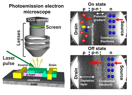
Organic p–n junction transistors show markedly large negative resistances even at room temperature. They clarified the origin of negative resistance using photoemission electron microscopy. They found that a steep potential gradient at the lateral p–n interface enhanced the electron conduction. In contrast, the conduction was suppressed when n-type or p-type semiconductor layer was completely depleted.
This achievement was made by a collaborative work between NIMS, University of Tsukuba and KEK.

Article Information
| Title | Carrier Transport Mechanism in Organic Antiambipolar Transistors Unveiled by Operando Photoemission Electron Microscopy |
| Journal | Advanced Materials |
| Date | May 30, 2022 |
| DOI | doi.org/10.1002/adma.202201277 |
Contact information
Research Center for Materials Nanoarchitectonics (MANA)
National Institute for Materials Science
1-1 Namiki, Tsukuba, Ibaraki 305-0044 Japan
Phone: +81-29-860-4710
E-mail: mana-pr[AT]ml.nims.go.jp
1-1 Namiki, Tsukuba, Ibaraki 305-0044 Japan
Phone: +81-29-860-4710
E-mail: mana-pr[AT]ml.nims.go.jp