- Home
- > Research
- > Research Highlights
- > Vol. 69 Direct Growth of Germanene Mar・・・
 Research Highlights
[Vol. 69]
Direct Growth of Germanene Marks a Major Step for Electronic Device Fabrication
- Previous
- Index
- Next
15 Jul, 2021
A team at MANA has succeeded in the direct growth of h-BN-capped germanene on the surface of silver Ag(111). They believe this could be a promising technique for the fabrication of germanene-based electronic devices in the future.
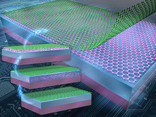
The MANA group grew the germanene at interfaces of graphene/Ag(111) and hexagonal boron nitride (h-BN)/Ag(111) by segregating germanium atoms. A simple annealing process in nitrogen (N2) or hydrogen/argon (H/Ar) at ambient pressure led to the formation of germanene, which indicated that ultrahigh-vacuum conditions are not necessary in this process. The resulting germanene was stable in air and uniform over the entire area covered with a van der Waals (vdW) material.
Germanene is one of a group of elements with two-dimensional honeycomb lattices, such as silicene, stanene and plumbene, which are collectively known as Xenes. These substances have electronic properties similar to those of graphene, including extremely high carrier mobility. In contrast to graphene, however, the honeycomb-lattice crystal structure of Xenes is not flat, but buckled, which results in their bandgaps being controllable by applying an electric field. Such bandgap controllability would provide a way to overcome the problem of gapless graphene for future electronic device applications. Thus, the utilization of Xenes in electronics is highly desirable.
In another important finding, the group discovered it was necessary to use a vdW material as a cap layer for their germanene growth method, since the use of an Al2O3 cap layer resulted in no germanene formation.
The results also prove that Raman spectroscopy in air is a powerful tool for characterizing germanene at an interface.
This research was carried out by Seiya Suzuki (ICYS Research Fellow, International Center for Young Scientists, ICYS-NAMIKI), Tomonobu Nakayama (MANA Principal Investigator, WPI-MANA) and their collaborators.
Reference
“Direct Growth of Germanene at Interfaces between Van der Waals Materials and Ag(111)”
Seiya Suzuki, Takuya Iwasaki, Kanishka H. De Silva, Shigeru Suehara, Kenji Watanabe, Takashi Taniguchi, Satoshi Moriyama, Masamichi Yoshimura, Takashi Aizawa, and Tomonobu Nakayama
Journal: Advanced Functional Materials [20 November 2020]
DOI : 10.1002/adfm.202007038
(MANA E-BULLETIN)
https://www.nims.go.jp/mana/ebulletin/
Affiliations
International Center for Materials Nanoarchitectonics (WPI-MANA), National Institute for Materials Science (NIMS), Namiki 1-1, Tsukuba, Ibaraki 305-0044, Japan
Contact information
Research Center for Materials Nanoarchitectonics (MANA)
National Institute for Materials Science
1-1 Namiki, Tsukuba, Ibaraki 305-0044 Japan
Phone: +81-29-860-4710
E-mail: mana-pr[AT]nims.go.jp
1-1 Namiki, Tsukuba, Ibaraki 305-0044 Japan
Phone: +81-29-860-4710
E-mail: mana-pr[AT]nims.go.jp