- Home
- > Research
- > Research Highlights
- > Vol. 50 Porous Structure of a Layered ・・・
 Research Highlights
[Vol. 50]
High-Performance Solar Cells Based on Silicon Nanopencil Structures
- Previous
- Index
- Next
16 Jul, 2019
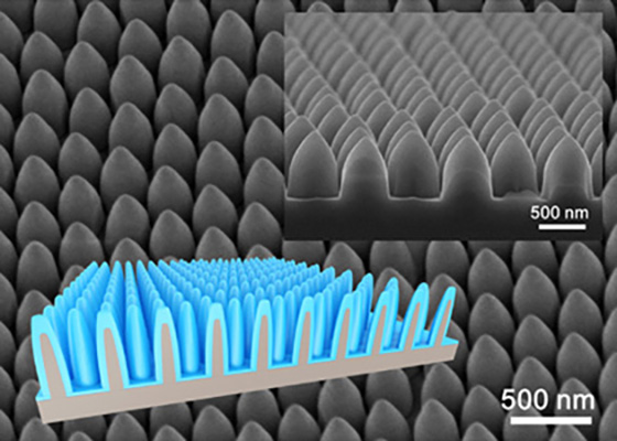
Figure: Nanowire array structures are called moss eye structures, which become black color due to the suppression of the light reflectance. Solar light energy create electrons and holes in nanowire structures and these electrons and holes are effectively separated by pn junction, resulting in high performance PV cells.
Solar cells are an important alternative energy source. The traditional solar-cell material of choice is crystalline silicon, which enables high power conversion efficiency, is stable, and has a well-established manufacturing process. Drawbacks with crystalline silicon are the high production cost and its fundamental efficiency limit. Now, Naoki Fukata at the International Center for Materials Nanoarchitectonics, National Institute for Materials Science, Tsukuba, Japan, and colleagues have fabricated a high-efficiency solar-cell material also based on silicon but with a significantly lower production cost. This work was done in collaboration with Oji Holdings Corporation.
The material consists of nano-sized pencil-shaped silicon rods — silicon nanopencils (SiNPs) — all aligned in one direction, etched out on a silicon wafer. The researchers used a combination of colloidal lithography and plasma reactive ion etching techniques. In colloidal lithography, a pattern is synthesized on a material by putting an ordered arrangement of colloidal particles on it; subsequent irradiation and removal of excess colloidal material then results in the patterned structure. In plasma reactive ion etching, material is etched away by using a chemically reactive plasma.
The obtained SiNP arrays where then made into proper solar cells with channels of silver between areas of SiNPs. When studying the conversion efficiency of their devices, Fukata and colleagues noted that the plasma etching process led to the development of too many defects, lowering device performance. To overcome this issue, the scientists applied a chemical polish etching method, which leads to a smooth device surface and better performance characteristics.
The researchers experimented with different structural parameters. In particular, they looked at the influence of the distance (pitch) between individual SiNPs, and so the density of SiNPs on the substrate. By also considering different silicon wafer thicknesses, they were able to obtain a maximum power conversion efficiency of 14.3%.
Further structural optimization of SiNP-based solar cells could lead to even better performance characteristics of devices of the type investigated by Fukata and colleagues. Quoting the scientists: “This high-performance device holds considerable potential for solar cell production on an industrial scale.”
Reference
“Fabrication of high-performance ordered radial junction silicon nanopencil T solar cells by fine-tuning surface carrier recombination and structure morphology”
Junyi Chen, Thiyagu Subramani, Wipakorn Jevasuwan, Kotaro Dai, Kei Shinotsuka, Yoshihisa Hatta, Naoki Fukata
Journal : Nano Energy 56, 604 (2019).
DOI : 10.1016/j.nanoen.2018.12.002
Junyi Chen, Thiyagu Subramani, Wipakorn Jevasuwan, Kotaro Dai, Kei Shinotsuka, Yoshihisa Hatta, Naoki Fukata
Journal : Nano Energy 56, 604 (2019).
DOI : 10.1016/j.nanoen.2018.12.002
Affiliations
International Center for Materials Nanoarchitectonics (WPI-MANA), National Institute for Materials Science (NIMS), Namiki 1-1, Tsukuba, Ibaraki 305-0044, Japan
Contact information
Research Center for Materials Nanoarchitectonics (MANA)
National Institute for Materials Science
1-1 Namiki, Tsukuba, Ibaraki 305-0044 Japan
Phone: +81-29-860-4710
E-mail: mana-pr[AT]nims.go.jp
1-1 Namiki, Tsukuba, Ibaraki 305-0044 Japan
Phone: +81-29-860-4710
E-mail: mana-pr[AT]nims.go.jp