 Press Release 2012
Development of Novel Conduction Control Technique for Graphene
Realizes a Room Temperature Operation Switching Transistor by Helium Ion Irradiation
24 Sep, 2012
A team of Dr. Shu Nakaharai (GNC, AIST; Researcher) and colleague with Dr. Kazuhito Tsukagoshi (WPI-MANA, PI) developed a novel technique for controlling the electrical conductivity of graphene.
In the technique developed in this research, a helium ion beam is irradiated on graphene using a helium ion microscope to artificially introduce a low concentration of crystal defects, and it becomes possible to modulate the conduction of electrons and holes in the graphene by applying a voltage to the gate electrode. Although this phenomenon of conduction control by introduction of crystal defects had been predicted theoretically, there were no experimental development in which on/off operation at room temperature was achieved experimentally. It would be possible to introduce the technique developed in this work in the existing framework of production technology, including large area wafers.
In the technique developed in this research, a helium ion beam is irradiated on graphene using a helium ion microscope to artificially introduce a low concentration of crystal defects, and it becomes possible to modulate the conduction of electrons and holes in the graphene by applying a voltage to the gate electrode. Although this phenomenon of conduction control by introduction of crystal defects had been predicted theoretically, there were no experimental development in which on/off operation at room temperature was achieved experimentally. It would be possible to introduce the technique developed in this work in the existing framework of production technology, including large area wafers.
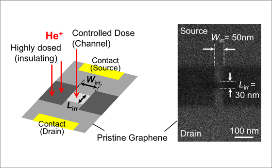
Fig. 1: He ion micrograph of fabricated device. The central Wirr×Lirr region was irradiated with He ion beam at controlled dose, and the conductivity of this region was investigated.

Fig. 2: Device characteristics of He ion irradiated graphene at room temperature. (Inset) Drain bias dependence of drain current and conductance.
Further information
Affiliation
Shu Nakahara1, Tomohiko Iijima2, Shinichi Ogawa3, Shingo Suzuki1, Songlin Li4, Hisao Miyazaki4, Tsukagoshi4, Shintaro Sato1, Naoki Yokoyama1
- 1.Nanoelectronics Research Institute, Collaborative Research Team Green Nanoelectronics Center (GNC), National Institute of Advanced Industrial Science and Technology (AIST)
- 2.Nanoelectronics Research Institute (ICAN), AIST
- 3.Innovation Center for Advanced Nanodevices (NeRI), AIST
- 4.International Center for Materials Nanoarchitectonics (WPI-MANA), National Institute for Materials Science (NIMS)
Contact information
For more detail about research
Collaborative Research Team Green Nanoelectronics Center, AIST
Naoki Yokoyama, Leader, Collaborative Research Team
mail: <yokoyama.naoki aist.go.jp>
TEL: +81-29-849-1607
FAX: +81-29-849-1186
Collaborative Research Team Green Nanoelectronics Center, AIST
Shintaro Sato, Group Leader, Collaborative Research Team
E-mail: <shintaro.satoaist.go.jp>
TEL: +81-29-849-1485
International Center for Materials Nanoarchitectonics (WPI-MANA),
National Institute for Materials Science (NIMS)
Kazuhito Tsukagoshi, Principal Investigator
mail: <TSUKAGOSHI.Kazuhitoinims.go.jp>
Naoki Yokoyama, Leader, Collaborative Research Team
mail: <yokoyama.naoki
aist.go.jp>TEL: +81-29-849-1607
FAX: +81-29-849-1186
Collaborative Research Team Green Nanoelectronics Center, AIST
Shintaro Sato, Group Leader, Collaborative Research Team
E-mail: <shintaro.sato
aist.go.jp>TEL: +81-29-849-1485
International Center for Materials Nanoarchitectonics (WPI-MANA),
National Institute for Materials Science (NIMS)
Kazuhito Tsukagoshi, Principal Investigator
mail: <TSUKAGOSHI.Kazuhitoi
nims.go.jp>For general inquiry
Public Relations Department, AIST
Email: press-mlaist.go.jp
TEL:+81-29-862-6216
FAX:+81-29-862-6212
Public Relations Office, NIMS
Email: prnims.go.jp
TEL:+81-29-859-2026
FAX:+81-29-859-2017
Email: press-ml
aist.go.jpTEL:+81-29-862-6216
FAX:+81-29-862-6212
Public Relations Office, NIMS
Email: pr
nims.go.jpTEL:+81-29-859-2026
FAX:+81-29-859-2017